Gallium nitride-based compound semiconductor lihgt-emitting device

A light-emitting device, gallium nitride-based technology, applied in the direction of semiconductor devices, electrical components, circuits, etc., can solve problems such as inability to improve light emission output, internal quantum efficiency reduction, etc., to achieve large light emission output, good crystallinity, Effect of Excellent Light Extraction Efficiency

Active Publication Date: 2008-07-02
TOYODA GOSEI CO LTD
View PDF1 Cites 16 Cited by
  • Summary
  • Abstract
  • Description
  • Claims
  • Application Information

AI Technical Summary

Problems solved by technology

However, in prior art flip-chip electrodes, since the contact metal is also used as a reflective metal or the contact metal is extremely thin, the semiconductor surface must be processed to form depressions / protrusions on the reflective electrode surface
As mentioned earlier, if such a treatment is performed on the semiconductor surface, the internal quantum efficiency decreases and the light emission output cannot be improved as desired

Method used


Image

  • Gallium nitride-based compound semiconductor lihgt-emitting device
  • Gallium nitride-based compound semiconductor lihgt-emitting device
  • Gallium nitride-based compound semiconductor lihgt-emitting device

Examples


example 1

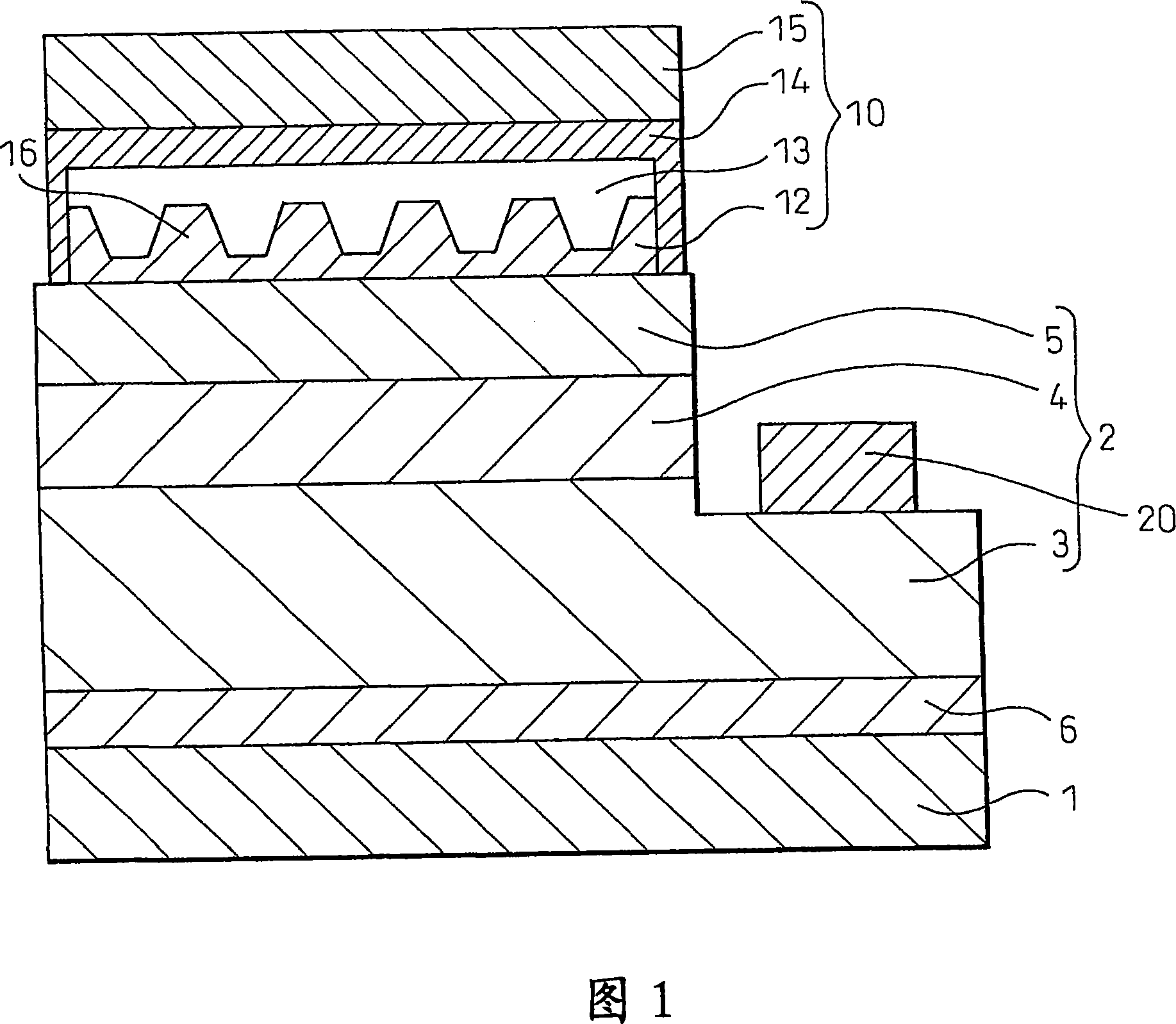
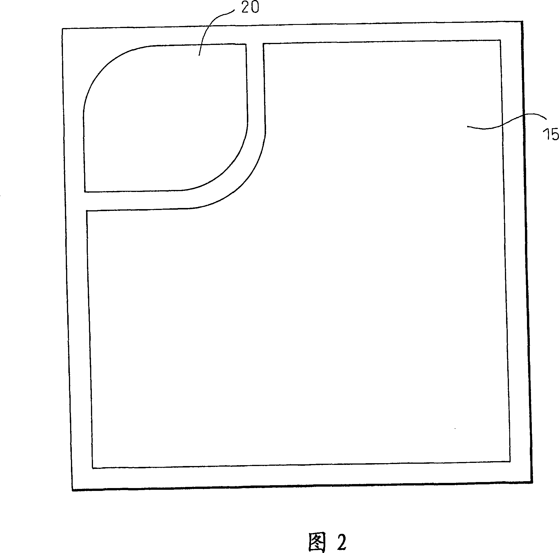
[0106] FIG. 1 is a schematic diagram showing a cross section of a gallium nitride-based compound semiconductor light-emitting device manufactured in this example, and FIG. 2 is a schematic diagram showing a plan view thereof. A gallium nitride-based compound semiconductor layer (2) is formed on a sapphire substrate (1) with an AlN buffer layer (6) interposed therebetween. The gallium nitride-based compound semiconductor layer (2) includes: an 8 μm thick undoped GaN base layer (base layer), a 2 μm thick Ge-doped n-type GaN contact layer, and a 0.02 μm thick Si-doped GaN contact layer. Miscellaneous n-type In 0.1 Ga 0.9 An n-type semiconductor layer (3) formed by an N-clad layer; five layers of 16 nm-thick Si-doped GaN barrier layers and five layers of 2.5 nm-thick In 0.06 Ga 0.94 The light-emitting layer (4) of the multi-quantum well structure constructed by N well layer and finally forming a barrier layer on top of the uppermost well layer; and by sequentially forming 0.01 ...

example 2

[0125] 11 is a schematic diagram showing a cross-section of a gallium nitride-based compound semiconductor light-emitting device manufactured in this example, and its plan view is the same as that shown in the schematic diagram of FIG. 2 in Example 1. FIG. As in Example 1, a gallium nitride-based compound semiconductor layer (2) was formed on a sapphire substrate (1) with an AlN buffer layer (6) interposed therebetween.

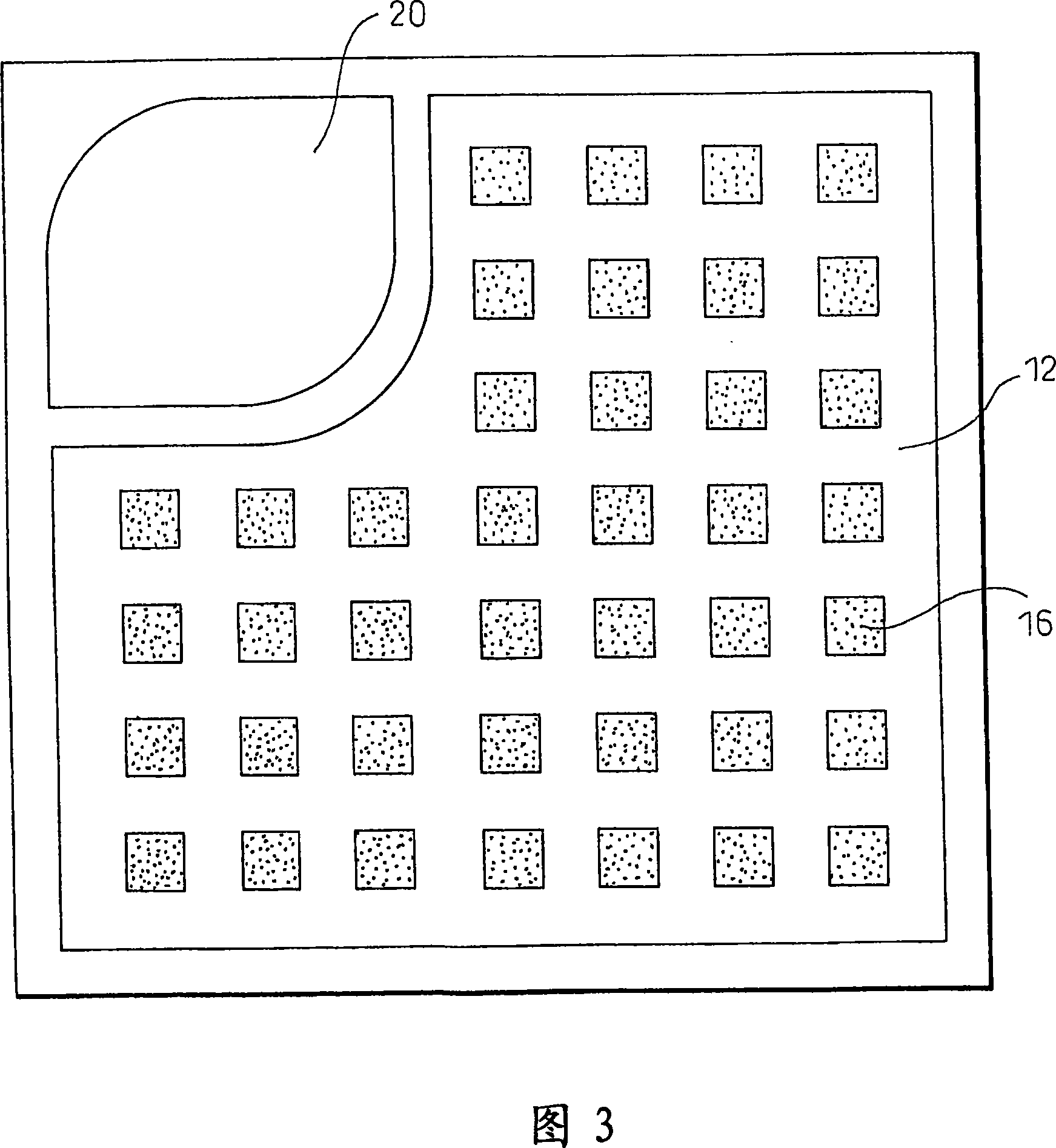
[0126] The structure of the positive electrode in this example is as follows. By forming the positive electrode contact layer (11) formed by 20nm thick ITO, by 180nm thick SiO 2 Formed transparent material layer (12), reflective metal layer (13) formed by 100nm thick Ag, covering layer (14) formed by 500nm thick Rh, and Au, Ti, Al, Ti and Au (thickness respectively The junction layer (15) of five-layer structure is 50nm, 20nm, 10nm, 100nm and 200nm), and the positive electrode (10) is formed on the p-type AlGaN contact layer. As in Example 1, in SiO 2 On t...


PUM


Abstract

An object of the present invention is to provide a gallium nitride-based compound semiconductor light emitting device having a reflective positive electrode configured to obtain excellent light extraction efficiency. The gallium nitride-based compound semiconductor light-emitting device of the present invention has a gallium nitride-based compound semiconductor layer structure on a substrate, and the gallium nitride-based compound semiconductor layer structure includes an n-type semiconductor layer, a light-emitting layer, and a p-type semiconductor layer, wherein The positive electrode disposed on the p-type semiconductor layer is a reflective positive electrode, and the reflective positive electrode includes a transparent material layer and a reflective metal layer formed on the transparent material layer.

Description

[0001] Cross References to Related Applications [0002] This application is based upon an application filed under 35 U.S.C. §111(a) pursuant to 35 U.S.C. §119(e)(1), requiring a provisional application filed under 35 U.S.C. §111(b) on July 12, 2005 Priority of No. 60 / 698,006. technical field [0003] The present invention relates to a gallium nitride-based compound semiconductor light-emitting device, and more particularly, to a flip-chip type gallium nitride-based compound semiconductor light-emitting device having a reflective positive electrode. Background technique [0004] In recent years, GaN-based compound semiconductor materials have attracted attention as semiconductor materials for short-wavelength light-emitting devices. GaN-based compound semiconductors are fabricated on various oxide and III-V compound substrates including single crystal sapphire by using methods such as metal organic chemical vapor deposition (MOCVD) or molecular beam epitaxy (MBE). [0005...

Claims


Application Information

Patent Timeline
Patent Type & Authority Applications(China)
IPC IPC(8): H01L33/00H01L33/22H01L33/32H01L33/38H01L33/40
Inventor 三木久幸篠原裕直龟井宏二
Owner TOYODA GOSEI CO LTD
Why Eureka
Try Eureka