Compound semiconductor light-emitting device and method of producing same

A light-emitting device and compound technology, which is applied in the field of pn junction compound semiconductor light-emitting devices, can solve problems such as difficult to obtain ohmic contact, and achieve the effect of reliable formation

Inactive Publication Date: 2007-04-11
SHOWA DENKO KK
View PDF5 Cites 0 Cited by
  • Summary
  • Abstract
  • Description
  • Claims
  • Application Information

AI Technical Summary

Problems solved by technology

However, these oxide films are difficult to obtain with III-V compound semiconductors such as aluminum gallium indium phosphide mixed crystals (Al X Ga 1-X ) Y In 1-Y Reliable ohmic contact of P
[0031] Thus, even when the medium passing through any of the above-mentioned transparent oxide films will, for example, have a transparent substrate sapphire (α-Al 2 o 3 single crystal), glass, titanium dioxide (TiO 2 ), or magnesium oxide (MgO) is bonded to the laminated structure, in the manufactured LED, it is difficult for the device operating current to diffuse over a wide area of ​​the laminated structure through the medium of the transparent substrate, which is problematic

Method used


Image

  • Compound semiconductor light-emitting device and method of producing same
  • Compound semiconductor light-emitting device and method of producing same
  • Compound semiconductor light-emitting device and method of producing same

Examples


example 1

[0169] The present invention will be described in detail by Example 1 below, in which a conductor layer made of undoped p-type boron arsenic phosphide and a light-transmitting substrate made of glass material are bonded together to form a pn junction compound semiconductor light emitting device.

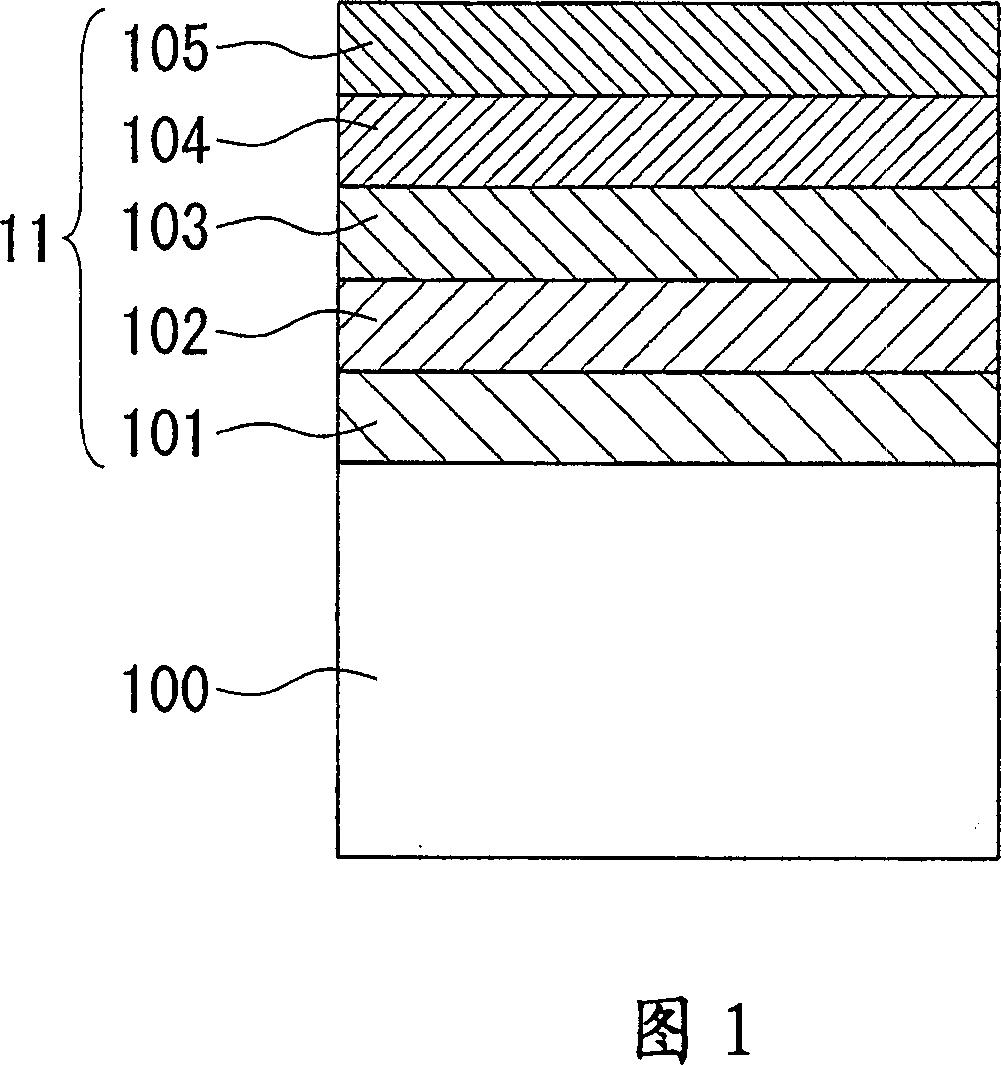
[0170] FIG. 1 is a schematic cross-sectional view of an exemplary stacked structure 11 having a pn junction double hetero (DH) junction structure and formed on a crystal substrate.

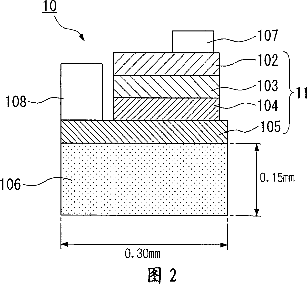
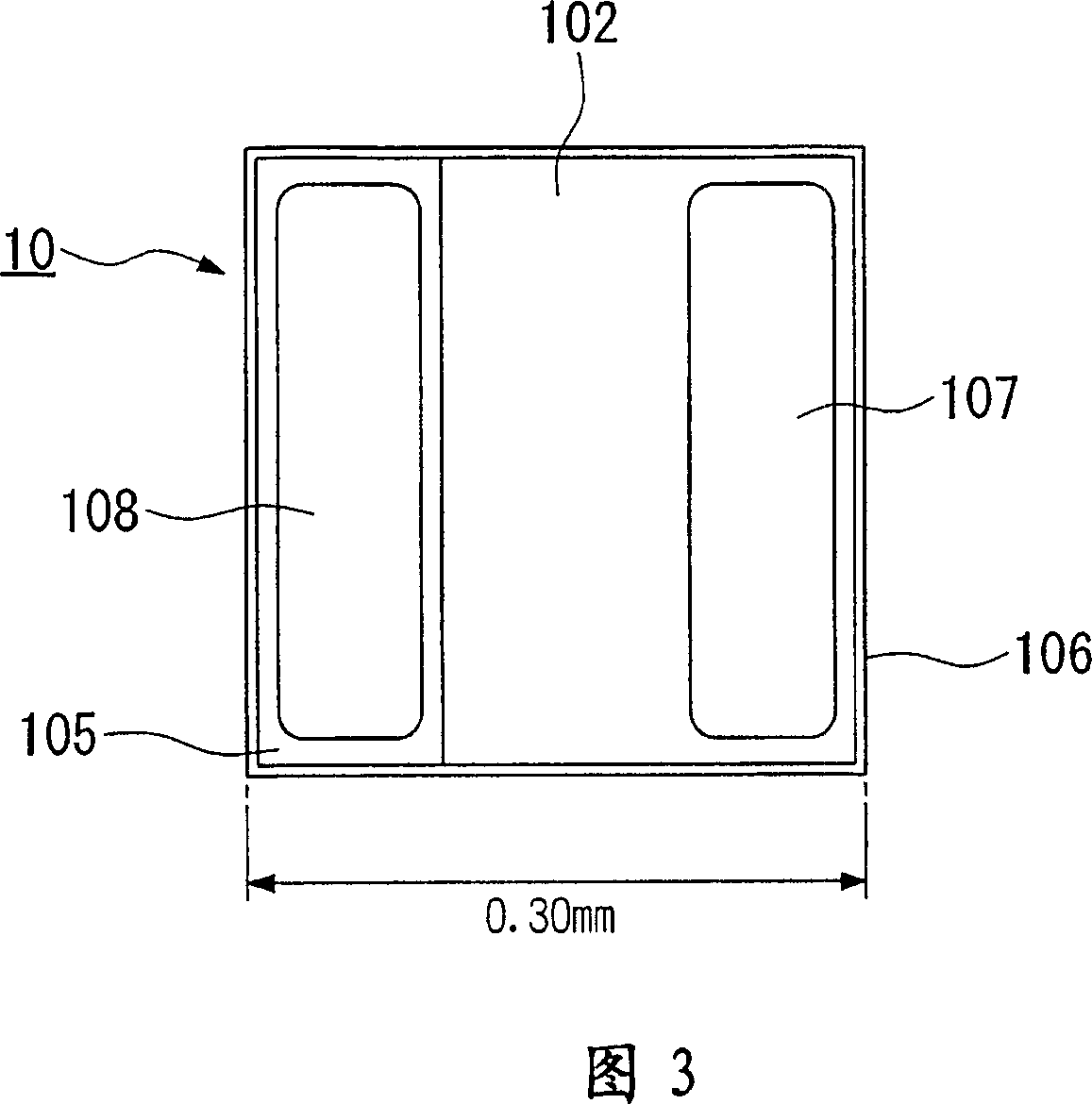
[0171] First, the laminated structure 11 for forming a pn junction compound semiconductor light emitting device 10 (hereinafter this device may be referred to as an LED chip) is formed through the following procedures.

[0172] The stacked structure 11 is formed by sequentially stacking the following layers on the (100) crystal plane of a zinc (Zn)-doped p-type gallium arsenide (GaAs) single crystal substrate 100: a zinc-doped p-type GaAs buffer layer 101, Aluminum gallium indium phosphide mixed crystal ...

example 2

[0206] The difference between the LED chip 20 and the LED of Example 1 is that an undoped n-type boron phosphide layer is provided as the conductor layer 205 .

[0207] The present invention will be described by Example 2 below. The same constituent members as employed in Example 1 are denoted by the same reference numerals.

[0208] 5 is a schematic cross-sectional view of an exemplary LED lamp 22 including the LED chip 20 of Example 2. As shown in FIG.

[0209] In a similar manner to Example 1, the constituent layers 101 to 104 of the laminated structure 21 except the conductor layer 205 were formed on the single crystal substrate 100 .

[0210] Next, an undoped n-type boron phosphide (BP) layer is formed on the upper cladding layer 104 as the conductor layer 205 .

[0211] At 800 ° C, by atmospheric pressure (close to atmospheric pressure) metal organic chemical vapor deposition (MOCVD) method, using triethylborane (molecular formula: (C 2 h 5 ) 3 B) as a source of bor...


PUM

PropertyMeasurementUnit
Thicknessaaaaaaaaaa
Thicknessaaaaaaaaaa
Thermal expansion coefficientaaaaaaaaaa

Abstract

A pn-junction compound semiconductor light-emitting device is provided, which comprises a stacked structure including a light-emitting layer composed of an n-type or a p-type aluminum gallium indium phosphide and a light-permeable substrate for supporting the stacked structure, and the stacked structure and the light-permeable substrate being joined together, wherein the stacked structure includes an n-type or a p-type conductor layer, the conductor layer and the substrate are joined together, and the conductor layer is composed of a Group 111-V compound semiconductor containing boron.

Description

[0001] Cross References to Related Applications [0002] Priority is claimed from Japanese Patent Application No. 2004-095145 filed March 29, 2004, the contents of which are incorporated herein by reference. This application also claims priority to US Provisional Application 60 / 559,429, filed April 6, 2004, under 35 U.S.C. §119(e)(1). technical field [0003] The present invention relates to a pn junction compound semiconductor light emitting device having a laminated structure including a light emitting layer composed of aluminum gallium indium phosphide mixed crystal (AlGaInP), and more particularly, to a pn junction compound semiconductor light emitting device obtaining high emission intensity. Background technique [0004] It is known to have a mixed crystal of aluminum gallium indium phosphide (component molecular formula: (Al X Ga 1-X ) Y In 1-Y P, 0≤X≤1) composed of a light-emitting diode (hereinafter also referred to as LED) with a light-emitting layer vapor-grow...

Claims


Application Information

Patent Timeline
IPC IPC(8): H01L33/00H01L33/16H01L33/30H01L33/40H01L33/56H01L33/62
CPCH01L33/30H01L2224/13H01L2224/48091H01L2224/48464H01L2224/49107H01L2224/73265
Inventor 竹内良一锅仓互宇田川隆
Owner SHOWA DENKO KK
Why Eureka
Try Eureka