Substrate for an organic light-emitting device and method for manufacturing the same
a technology of organic light-emitting devices and substrates, which is applied in the direction of sustainable manufacturing/processing, final product manufacturing, instruments, etc., can solve the problems of diode internal light extraction efficiency decline, diode electrical instability, surface becomes uneven like the coated surface, etc., to improve light extraction efficiency, improve the effect of light extraction efficiency and excellent degree of planarization
- Summary
- Abstract
- Description
- Claims
- Application Information
AI Technical Summary
Benefits of technology
Problems solved by technology
Method used
Image
Examples
example 1
Manufacture of Substrate for Organic Light Emitting Diode
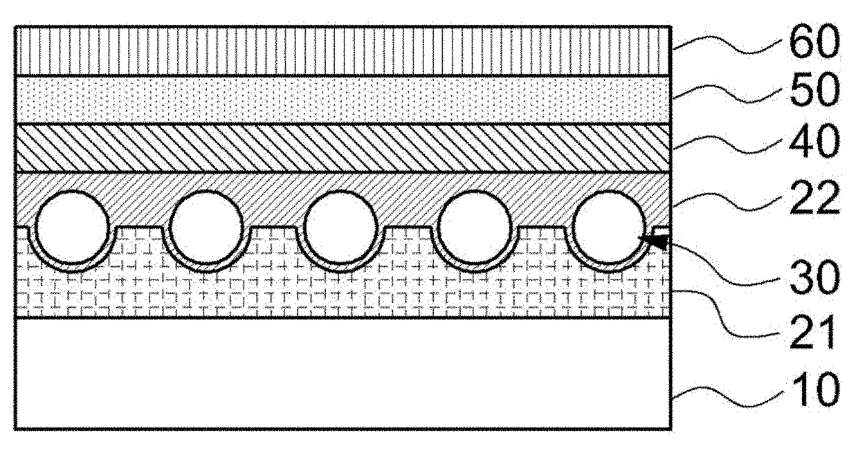
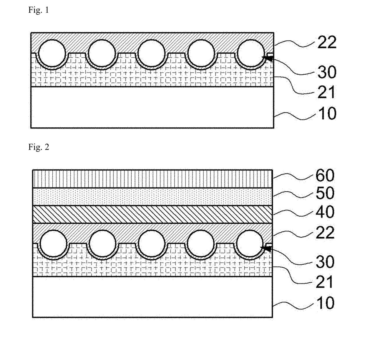
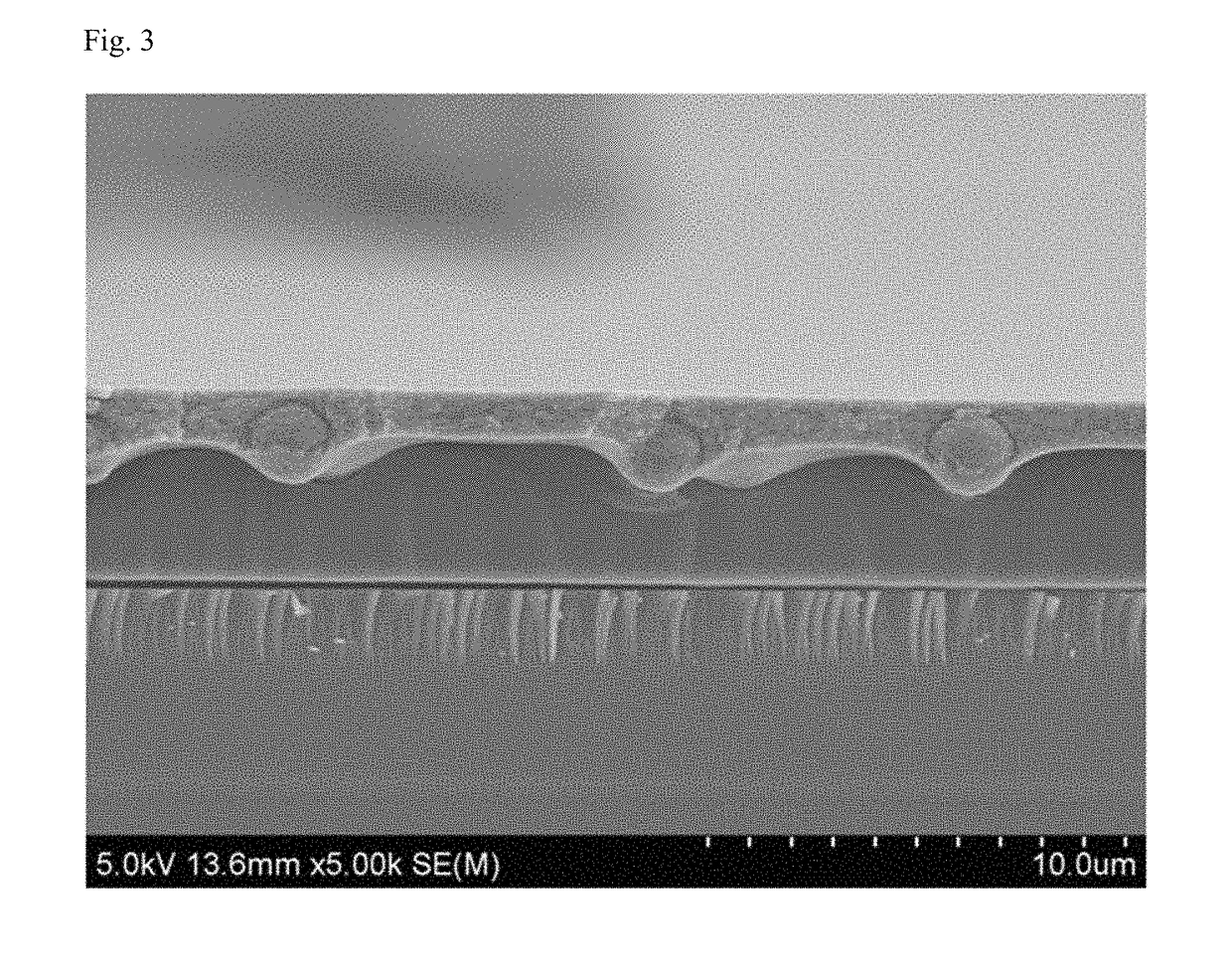
[0058]A coating solution was prepared by sufficiently mixing 1 g of polymer beads (XX75BQ, diameter: 3 μm, Sekisui) having a refractive index of approximately 1.52 in 10 g of a UV curable organic binder (TYT-80-01, solid content: 25 wt %, Toyo ink) in which a high refractive filler is dispersed. Afterward, the coating solution was coated on a surface of a polyester film (PET film) which was not treated with a primer using a coater (#6 Meyer bar coater). Subsequently, the coated coating solution was dried at 100° C. for 2 minutes and cured with an energy of 1 J / cm2 using a UV curing system, thereby manufacturing a film. Separately, a suitable amount of UV curable adhesive (NOA65, Norland Products Inc.) was dropped on a glass substrate for an organic light emitting diode (OLED), the coated coating film was covered such that the coating layer faced the glass substrate, and the polyester film was pressed with a rubber roller to la...
example 2
[0062]A substrate and an OLED formed on a planarized surface thereof were manufactured by the same method as described in Example 1, except that the number of polymer beads was changed to 1.5 g in preparation of a coating solution.
experimental example 1
Measurement of Roughness
[0065]Degrees of planarization were measured with respect to the substrates manufactured in Examples 1 and 2 and Comparative Examples 1 and 2. Particularly, the maximum height roughness was measured with respect to surfaces of the substrates manufactured in Examples and Comparative Examples, which were opposite to a transparent glass substrate. The maximum height roughness was obtained by measuring a difference between the maximum height and the minimum height of the manufactured sample, which was measured within a 10×10 μm2 region. Measurement results were shown in Table 2.
[0066]
TABLE 2ComparativeExample 1Example 2Example 1Maximum height0.30.161.4roughness (μm)
[0067]Referring to Table 2, it can be seen that the planarized surfaces of the substrates in Examples 1 and 2 according to an exemplary embodiment of the present invention have a maximum height roughness of within 1 μm, but that in Comparative Example 2 is considerably increased in maximum height rough...
PUM
 Abstract
Description
Claims
Application Information


