Gallium-nitride-based compound semiconductor light emitting element and its manufacturing method

A light-emitting device, GaN-based technology, applied in semiconductor/solid-state device manufacturing, semiconductor devices, electrical components, etc., can solve problems such as troublesome processes, decreased production efficiency, complexity, etc., to achieve high output power, interference effect suppression, Improve the effect of light focusing

Active Publication Date: 2009-12-23
TOYODA GOSEI CO LTD
View PDF6 Cites 0 Cited by
  • Summary
  • Abstract
  • Description
  • Claims
  • Application Information

AI Technical Summary

Problems solved by technology

[0012] However, the gallium nitride-based compound semiconductor light-emitting device manufactured by the method described in Patent Document 1 has the disadvantage of causing an interference effect in an uneven pattern formed on a semiconductor surface by a mask patterning method and intensifying only light of a specific wavelength. question
[0013] In addition, since a fine mask patterning method is required in the method of roughening the surface of the semiconductor layer, a complicated and cumbersome process must be employed in the process, and production efficiency decreases

Method used


Image

  • Gallium-nitride-based compound semiconductor light emitting element and its manufacturing method
  • Gallium-nitride-based compound semiconductor light emitting element and its manufacturing method
  • Gallium-nitride-based compound semiconductor light emitting element and its manufacturing method

Examples


example 1

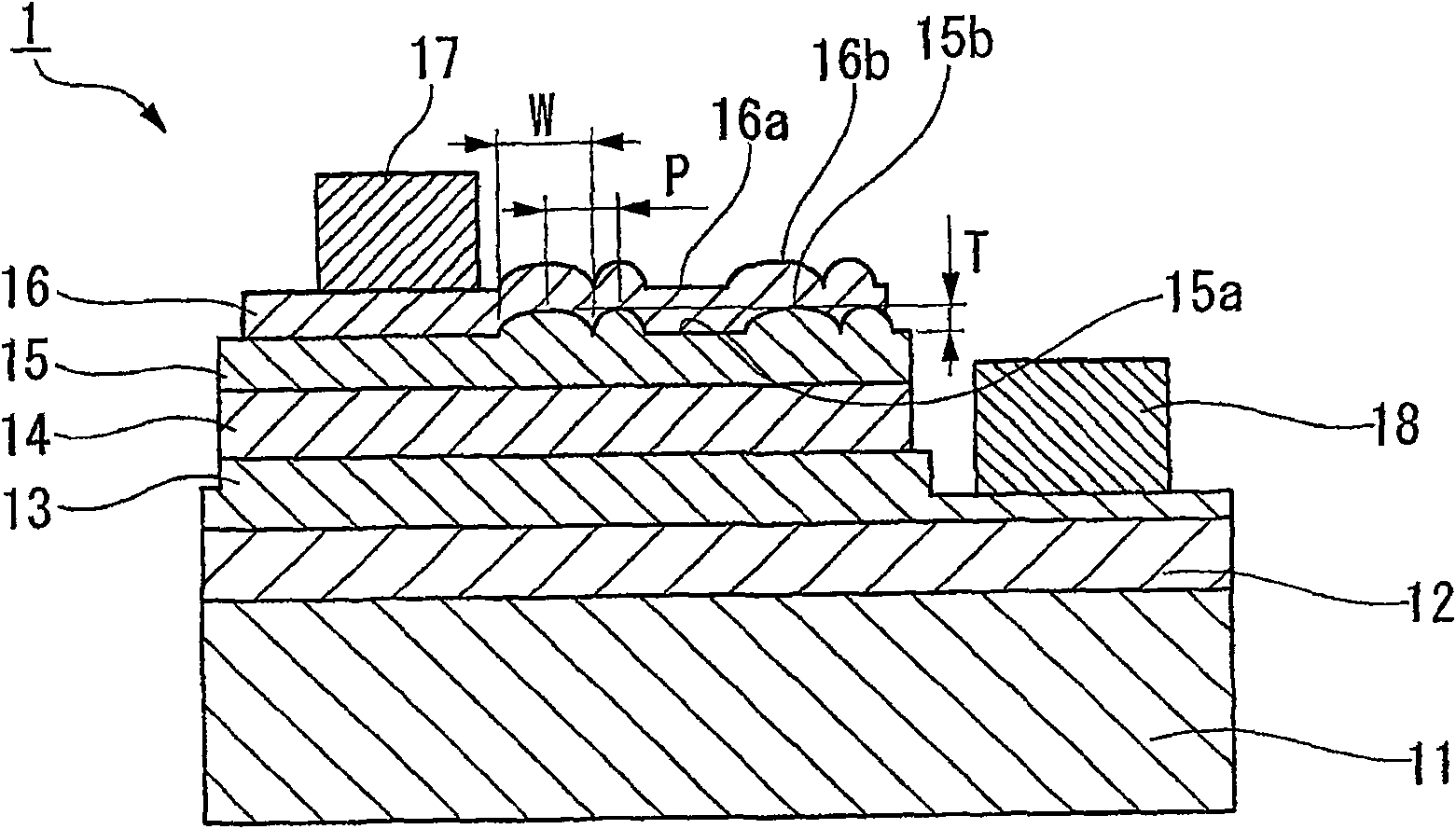
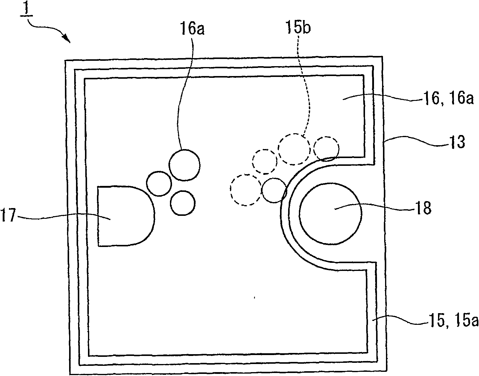
[0136] figure 1 A schematic diagram showing a cross-section of a gallium nitride-based compound semiconductor light-emitting device fabricated as an example, while figure 2 A schematic plan view is shown.

[0137] (Manufacture of Gallium Nitride-based Compound Semiconductor Light-Emitting Devices)

[0138] A gallium nitride-based compound semiconductor layer is laminated on a substrate 1 made of sapphire through a buffer layer 12 made of AlN. The gallium nitride-based compound semiconductor layer includes: an n-type semiconductor layer in which an 8-μm-thick lower layer made of undoped GaN, a 2-μm-thick Ge-doped n-type GaN contact layer, and a 0.02-μm-thick n-type GaN contact layer are sequentially stacked. In 0.1 Ga 0.9 N cladding layer; five layers of 16nm thick Si-doped GaN barrier layer and 2.5nm thick In 0.06 Ga 0.94 N well layer, and finally, light emitting layer 14 having a multi-quantum well structure provided with a barrier layer; and p-type Al doped with Mg by...

example 2-10

[0163] Materials used for the metal fine particles are shown in Table 1. A point under which heat treatment was performed at the heating temperature shown in Table 1 was excluded, and a gallium nitride-based compound semiconductor light-emitting device was produced similarly to Example 1.

example 11

[0165] A spot under which an uneven pattern consisting of protrusions was not formed on the surface of the p-type semiconductor layer was excluded, and a gallium nitride-based compound semiconductor light-emitting device was fabricated similarly to Example 1.

[0166] Examples 12 to 13

[0167] Points under which the mean value and standard deviation of the protrusions on the surface of the p-type semiconductor layer became the same as the values ​​shown in Table 1 were excluded, and a gallium nitride-based compound semiconductor was produced similarly to Example 1 device.

[0168] Table 1 shows a list of conditions of the uneven shape, protrusion distance, and device characteristics of Examples 1 to 13 described above.

[0169]

[0170] From the evaluation results of device characteristics shown in Table 1, the average distance of the protrusions of the gallium nitride-based compound semiconductor light-emitting devices of Examples 1 to 10 in which a disordered uneven sur...


PUM


Abstract

The invention provides a gallium nitride-based compound semiconductor light emitting device with excellent light extraction efficiency and a manufacturing method thereof. A light-emitting device obtained from a gallium nitride-based compound semiconductor includes: a substrate; an n-type semiconductor layer 13, a light-emitting layer 14, and a p-type semiconductor layer 15 stacked sequentially on the substrate 11; The light-transmitting positive electrode 16; the positive electrode bonding pad 17 disposed on the light-transmitting positive electrode 16; and the negative electrode bonding pad 18 disposed on the n-type semiconductor layer 13, wherein on the surface 15a of the p-type semiconductor layer 15 A disordered uneven surface is formed on at least a portion of the .

Description

[0001] Cross References to Related Applications [0002] Priority is claimed from Japanese Patent Application No. 2005-258135 filed September 6, 2005 and Japanese Patent Application No. 2005-360291 filed December 14, 2005. This application is based on 35 U.S.C. § 111(a) under 35 U.S.C. § 119(e), requiring provisional application 60 / 716,963 filed September 15, 2005 under 35 U.S.C. § 111(b) and filed at Priority of provisional application 60 / 752,962 filed December 23, 2005. technical field [0003] The present invention relates to a gallium nitride-based compound semiconductor light-emitting device with particularly high output power and a manufacturing method thereof. Background technique [0004] In recent years, gallium nitride (GaN)-based compound semiconductor light-emitting devices have attracted attention as short-wavelength light-emitting devices. This nitrogen is formed on a substrate composed of various oxides or Group IH to Group V compounds starting from a sapphi...

Claims


Application Information

Patent Timeline
Patent Type & Authority Patents(China)
IPC IPC(8): H01L33/00H01L21/3065
Inventor 村木典孝篠原裕直大泽弘
Owner TOYODA GOSEI CO LTD
Why Eureka
Try Eureka