Wet oxidation process performed on a dielectric material formed from a flowable CVD process

a dielectric material and flowable technology, applied in the direction of basic electric elements, semiconductor/solid-state device manufacturing, electric apparatus, etc., can solve the problems of high manufacturing cost, low throughput of harp processes, and adversely affecting device performan

Active Publication Date: 2012-06-07
APPLIED MATERIALS INC
View PDF3 Cites 30 Cited by
  • Summary
  • Abstract
  • Description
  • Claims
  • Application Information

AI Technical Summary

Benefits of technology

[0057]Furthermore, the wet oxidation processing solution provides a low cost, fast and simple process so that the overall process complexity may be reduced while also reducing manufacturing cost and process cycle time. In one embodiment, the process time for the wet oxidation process performed on the substrate 400 may be controlled at between about 1 seconds and about 10 hours. Alternatively, the process time may also be controlled by observing the bonding structures formed in the oxidized dielectric material 412 until a desired percentage or atomic weight of the silicon-nitrogen and / or silicon-hydrogen bonding in the dielectric material 408 have been converted into the silicon-oxygen bonding. The bonding structure of the oxidized dielectric material 412 may be inspected or observed by FTIR, SIMS or XPS.

Problems solved by technology

However, as the limits of integrated circuit technology are pushed, the shrinking dimensions of interconnects in VLSI and ULSI technology have placed additional demands on processing capabilities.
One challenge regarding the manufacture of high aspect ratio trenches is avoiding the formation of voids during the deposition of dielectric material in the trenches.
However, as the aspect ratio increases, it becomes more likely that the opening of the trench will “pinch off”, forming a void within the trench.
However, this deposition technique often suffers from high film impurities as the liquid precursor used to fill in the trench may include contaminants that may adversely deteriorate on the electrical properties of the formed dielectric material which adversely affects device performance.
However, HARP processes often have low throughput, which results in high manufacturing cost.

Method used


Image

  • Wet oxidation process performed on a dielectric material formed from a flowable CVD process
  • Wet oxidation process performed on a dielectric material formed from a flowable CVD process
  • Wet oxidation process performed on a dielectric material formed from a flowable CVD process

Examples


Embodiment Construction

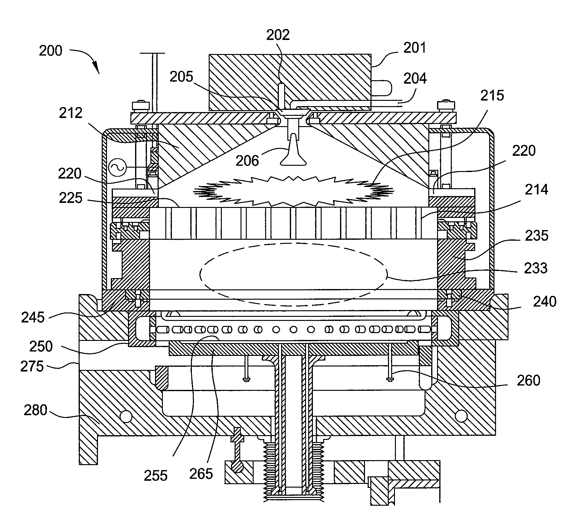
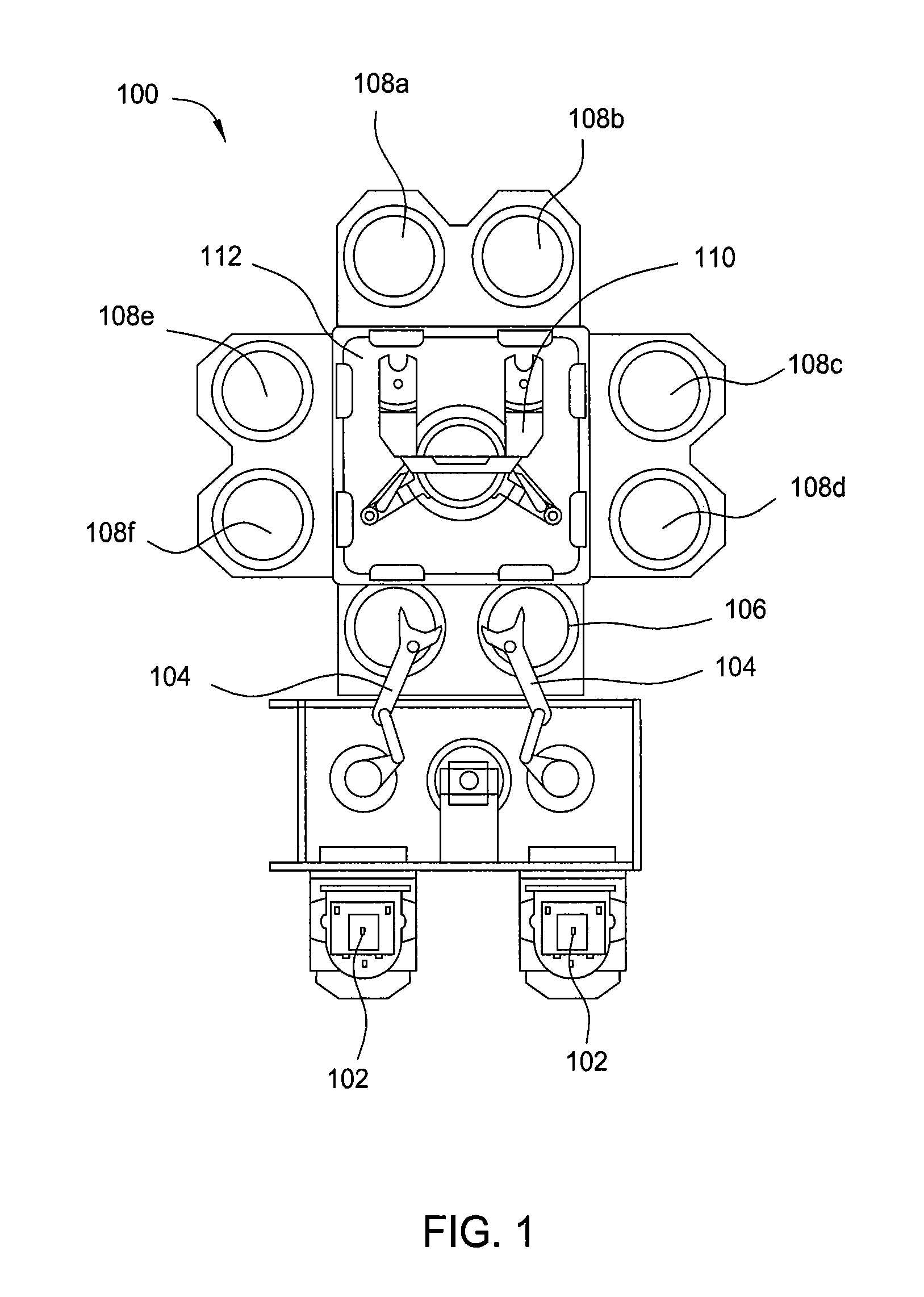
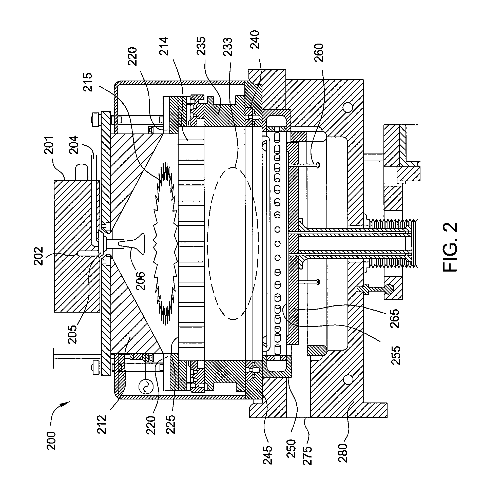
[0022]FIG. 1 is a top plan view of one embodiment of a processing tool 100 of deposition, baking and curing chambers according to disclosed embodiments. In the processing tool 100, a pair of FOUPs (front opening unified pods) 102 supply substrate substrates (e.g., 300 mm diameter wafers) that are received by robotic arms 104 and placed into load lock chambers 106. A second robotic arm 110 is disposed in a transfer chamber 112 coupled to the load lock chambers 106. The second robotic arm 110 is used to transport the substrates from the load lock chambers 106 to processing chambers 108a-f coupled to the transfer chamber 112.

[0023]The processing chambers 108a-f may include one or more system components for depositing, annealing, curing and / or etching a flowable dielectric film on the substrate wafer. In one configuration, two pairs of the processing chamber (e.g., 108c-d and 108e-f) may be used to deposit the flowable dielectric material on the substrate, and the third pair of processi...


PUM

PropertyMeasurementUnit
temperatureaaaaaaaaaa

Abstract

Methods of performing a wet oxidation process on a silicon containing dielectric material filling within trenches or vias defined within a substrate are provided. In one embodiment, a method of forming a dielectric material on a substrate includes forming a dielectric material on a substrate by a flowable CVD process, curing the dielectric material disposed on the substrate, performing a wet oxidation process on the dielectric material disposed on the substrate, and forming an oxidized dielectric material on the substrate.

Description

CROSS-REFERENCE TO OTHER APPLICATIONS[0001]This application is a continuation of co-pending U.S. Ser. No. 12 / 643,196, filed Dec. 21, 2009 which is herein incorporated by reference.BACKGROUND OF THE INVENTION[0002]1. Field of the Invention[0003]The invention relates to a method for processing substrates, such as semiconductor wafers, and more particularly, to a method for wet oxidizing a dielectric material disposed on a substrate.[0004]2. Description of the Related Art[0005]Reliably producing sub-half micron and smaller features is one of the key technologies for the next generation of very large scale integration (VLSI) and ultra large-scale integration (ULSI) of semiconductor devices. However, as the limits of integrated circuit technology are pushed, the shrinking dimensions of interconnects in VLSI and ULSI technology have placed additional demands on processing capabilities. Integrated circuits may include more than one million micro-electronic field effect transistors (e.g., c...

Claims


Application Information

Patent Timeline
Patent Type & Authority Applications(United States)
IPC IPC(8): H01L21/316
CPCH01L21/02343H01L21/02326
Inventor WANG, LINLINMALLICK, ABHIJIT BASUINGLE, NITIN K.
Owner APPLIED MATERIALS INC
Why Eureka
Try Eureka