System and Method for Analyzing an Electronics Device Including a Logic Analyzer

a logic analyzer and electronics device technology, applied in the field of embedded logic analyzers, can solve the problems of increasing the overall cost of the ic to unreasonable levels, the manufacturing cost of the ic to be substantially increased, etc., and achieve the effect of effective testing and debugging

Active Publication Date: 2012-06-07
LEXMARK INT INC
View PDF5 Cites 14 Cited by
  • Summary
  • Abstract
  • Description
  • Claims
  • Application Information

AI Technical Summary

Benefits of technology

[0012]Exemplary embodiments of the present disclosure overcome the shortcomings in known test systems and thereby satisfy a significant need for effectively testing and debugging an electronics device or system having a logic analyzer. In accordance with an exemplary embodiment, a technique is employed which takes advantage of time-division multiplexing (TDM) multiple signals across the same input bus to an ELA. An ELA conventionally includes or is associated with an input multiplexer to which candidate signals are routed, wherein a group of input signals selected by the input multiplexer is available for sampling and / or triggering an event during the test or debug operation. This input signal group selection is typically made before a test program is executed and remains static for the duration of a corresponding test or debug session. In order to provide more captured signals for a test or debug program, multiple input signal groups can be time division multiplexed over the same input bus. By changing the multiplexer selection signals dynamically during the program and capturing the selection signals along with the selected signals, test / debug software executed on a host computing device is then able to reconstruct the captured multiplexed input signals for presentation to a user without the user needing to know the particulars of the input signal group selection by the input multiplexer.

Problems solved by technology

In addition, the routing congestion from having a large number of signals routed to ELA 100 alone can make the IC containing ELA 100 either unroutable or cause the size and therefore manufacturing cost of the IC to undesirably substantially increase.
The size requirements for getting the desired amount of information to ELA 100 for selection thereby could increase the overall cost of the IC to unreasonable levels.

Method used


Image

  • System and Method for Analyzing an Electronics Device Including a Logic Analyzer
  • System and Method for Analyzing an Electronics Device Including a Logic Analyzer
  • System and Method for Analyzing an Electronics Device Including a Logic Analyzer

Examples


Embodiment Construction

[0038]Reference will now be made in detail to the exemplary embodiment(s) of the disclosure, as illustrated in the accompanying drawings. Whenever possible, the same reference numerals will be used throughout the drawings to refer to the same or like parts.

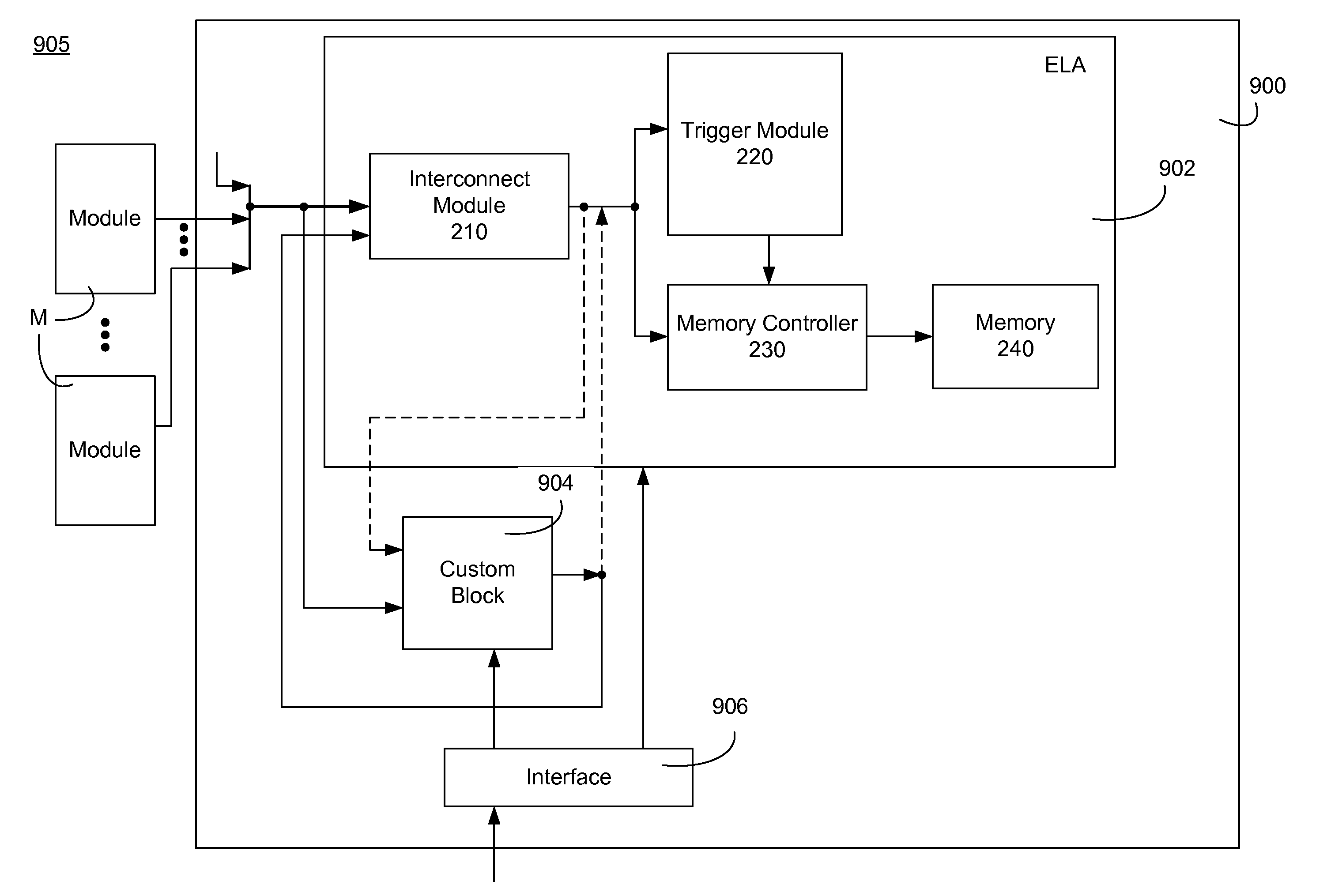
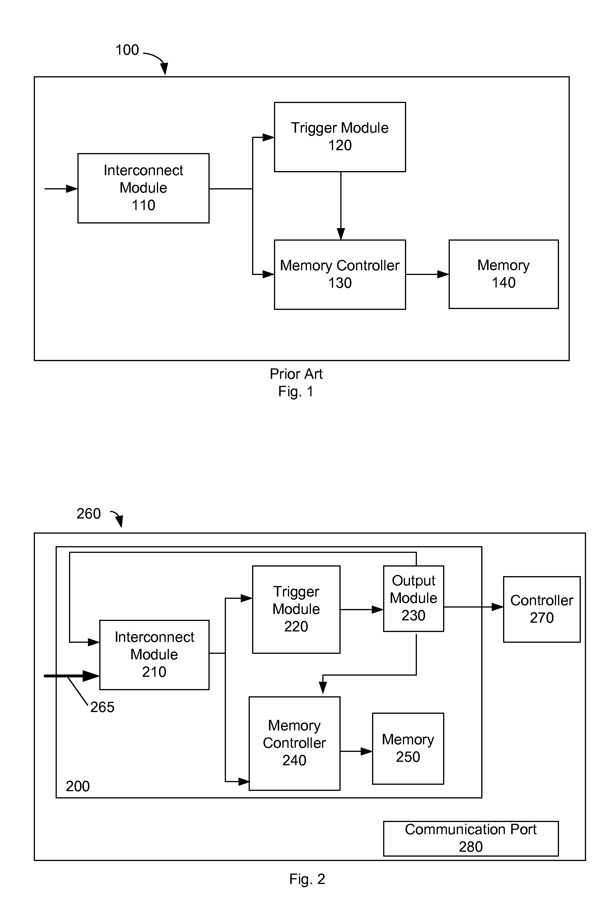
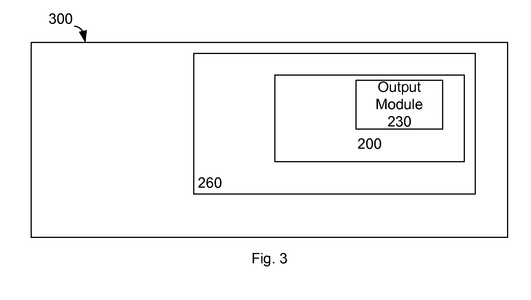
[0039]The present disclosure is directed to a programmable embedded logic analyzer included within an integrated circuit having enhanced analyzing and debugging capabilities. FIG. 2 illustrates one embodiment of an embedded logic analyzer (ELA) 200 disposed on an integrated circuit (IC) 260. The ELA 200 includes an interconnect module 210 that is programmable to select at least one of a plurality of candidate signals within the IC 260. The plurality of candidate signals selected by the interconnect module 210 may include at least one trigger signal and / or at least one signal to be sampled (i.e., a sampled signal). The interconnect module 210 routes the at least one trigger signal to a trigger module 220. The trigger module 220 det...


PUM


Abstract

A system for testing or debugging a device under test having an embedded logic analyzer. In one embodiment, the system includes software stored in non-transitory memory for testing a device under test having an embedded logic analyzer, the software program product having instructions which, when executed by a computing device associated with the device under test cause the computing device to reconstruct signals of interest in the device under test based at least in part upon signals captured by the embedded logic analyzer during the test or debug session, and cause the computing device to display the reconstructed signals of interest to a user of the computing device.

Description

CROSS REFERENCE TO RELATED APPLICATIONS[0001]Pursuant to 37 C.F.R. §1.78, this application is a continuation-in-part application and claims the benefit of the earlier filing date of application Ser. No. 12 / 983,016, filed Dec. 31, 2010, and entitled “A System and Method for Analyzing an Electronics Device Including a Logic Analyzer,” which itself application is a continuation-in-part application and claims the benefit of the earlier filing date of application Ser. No. 12 / 877,846, filed Sep. 8, 2010, and entitled “An Integrated Circuit Including a Programmable Logic Analyzer with Enhanced Analyzing and Debugging Capabilities,” and application Ser. No. 12 / 877,819, filed Sep. 8, 2010, and entitled “An Integrated Circuit Including a Programmable Logic Analyzer with Enhanced Analyzing and Debugging Capabilities and a Method thereof,” which are continuation-in-part applications of U.S. application Ser. No. 12 / 542,976, filed Aug. 18, 2009, entitled “An Integrated Circuit Including a Program...

Claims


Application Information

Patent Timeline
Patent Type & Authority Applications(United States)
IPC IPC(8): G01R31/3177G06F11/25
CPCG01R31/3177G06F11/2294G06F11/273G06F11/26G06F11/25
Inventor BAILEY, JAMES RAYCASE, CHRISTOPHER W.SHARPE, JAMES PATRICKWARD, JAMES ALANMARRA, III, MICHAEL ANTHONY
Owner LEXMARK INT INC
Why Eureka
Try Eureka