Photodetector circuit, input device, and input/output device

a photodetector circuit and input/output device technology, applied in the direction of electrical equipment, semiconductor devices, radio frequency controlled devices, etc., can solve the problems of large influence of the photodetector circuit and the value of optical data, and achieve the effect of suppressing parasitic capacitance on optical data in the photodetector circuit and reducing the cost of operation

Active Publication Date: 2012-06-14
SEMICON ENERGY LAB CO LTD
View PDF1 Cites 14 Cited by
  • Summary
  • Abstract
  • Description
  • Claims
  • Application Information

AI Technical Summary

Benefits of technology

[0019]According to one embodiment of the present invention, an adverse effect of parasitic capacitance on optical data in a photodetector circuit can be suppressed.

Problems solved by technology

However, a conventional photodetector circuit has a problem in that the value of optical data varies depending on parasitic capacitance.
In particular, in the conventional photodetector circuit, current flowing through the photoelectric conversion element is amplified with the use of the amplifier transistor, converted into voltage, and output as optical data; thus, the photodetector circuit is greatly affected even by small parasitic capacitance.

Method used


Image

  • Photodetector circuit, input device, and input/output device
  • Photodetector circuit, input device, and input/output device
  • Photodetector circuit, input device, and input/output device

Examples


embodiment 1

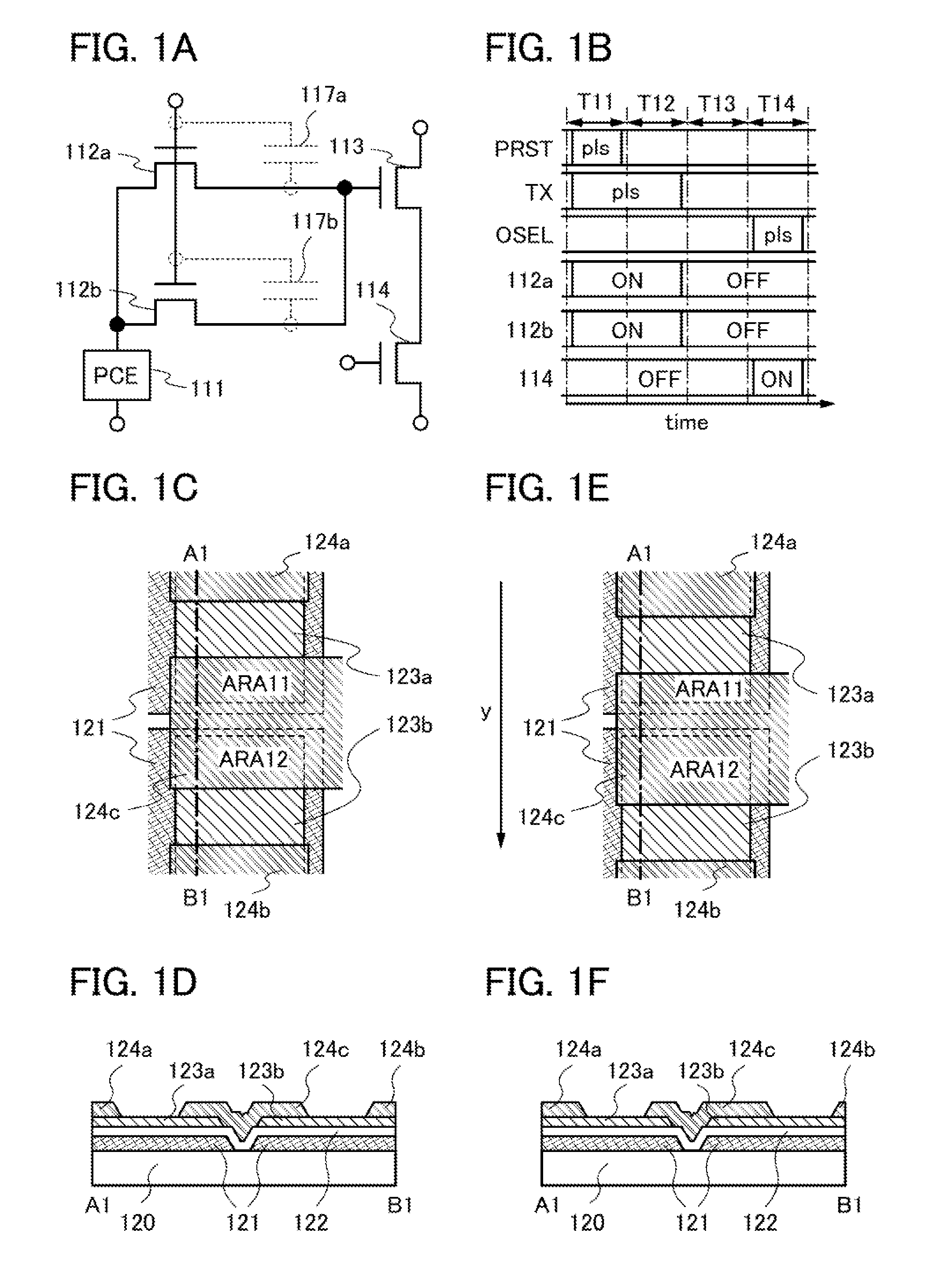
[0052]In this embodiment, an example of a photodetector circuit will be described.

[0053]The example of the photodetector circuit in this embodiment will be described with reference to FIGS. 1A to 1F.

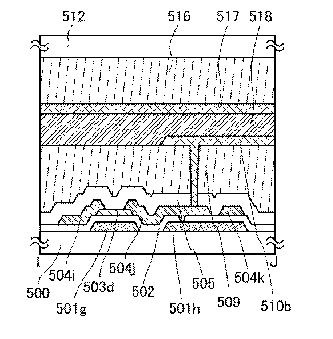
[0054]First, a structural example of the photodetector circuit in this embodiment will be described with reference to FIG. 1A.

[0055]The photodetector circuit illustrated in FIG. 1A includes a photoelectric conversion element 111, a transistor 112a, a transistor 112b, a transistor 113, and a transistor 114.

[0056]The transistor 112a the transistor 112b, the transistor 113, and the transistor 114 are field-effect transistors.

[0057]The photoelectric conversion element 111 includes a first current terminal and a second current terminal, and current. (also referred to as photocurrent) flows between the first current terminal and the second current terminal in accordance with the illuminance of incident light.

[0058]A photodetection reset signal (also referred to as a signal PRST) that is a puls...

embodiment 2

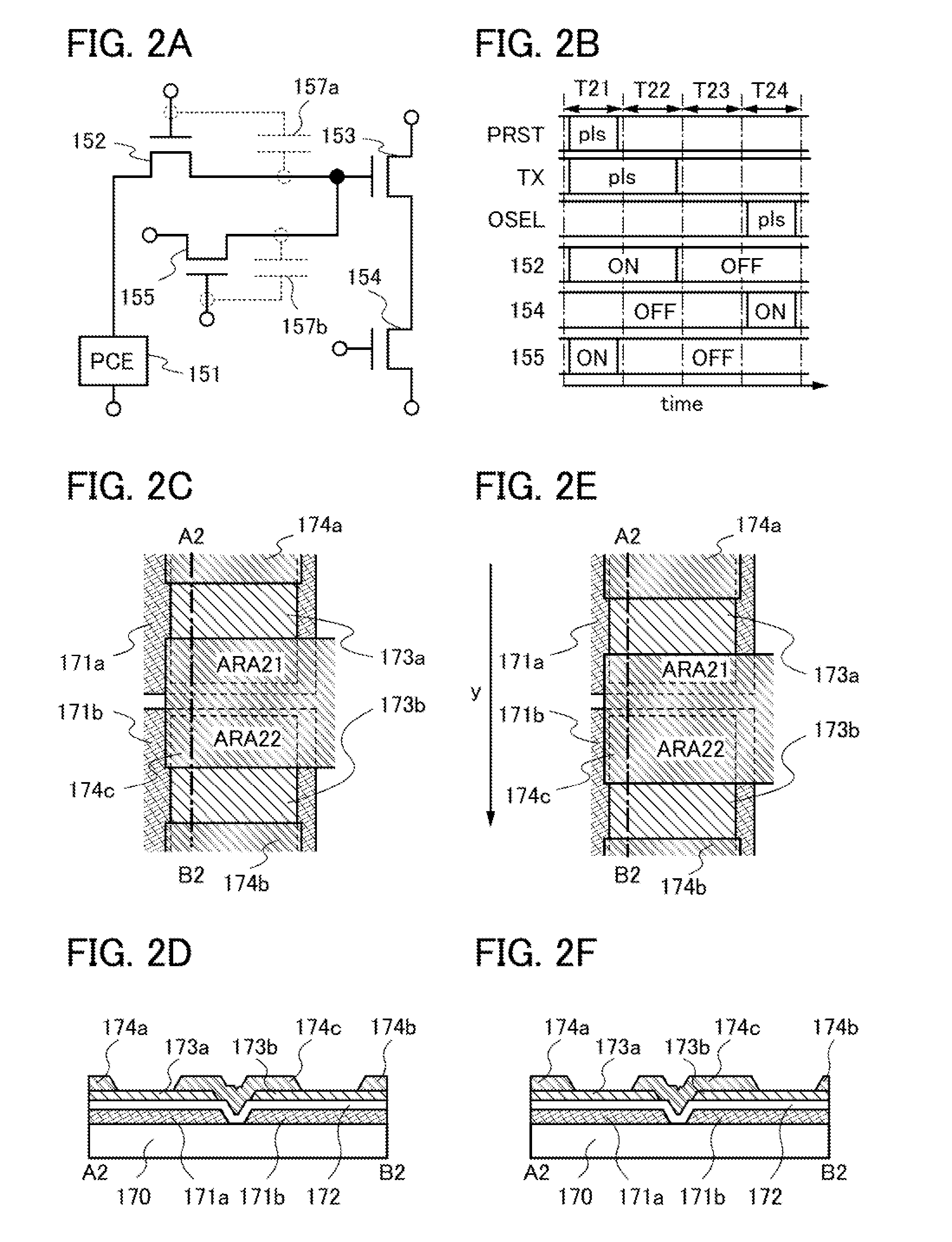
[0158]In this embodiment, an example of a photodetector circuit whose structure is partly different from that in Embodiment 1 will be described. Note that the description of the photodetector circuit in Embodiment 1 can be referred to as appropriate for the same portions as those in the photodetector circuit described in Embodiment 1.

[0159]The example of the photodetector circuit in this embodiment will be described with reference to FIGS. 2A to 2F.

[0160]First, a structural example of the photodetector in this embodiment is described with reference to FIG. 2A.

[0161]The photodetector circuit illustrated in FIG. 2A includes a photoelectric conversion element 151, a transistor 152, a transistor 153, a transistor 154, and a transistor 155.

[0162]The transistor 152, the transistor 153, the transistor 154, and the transistor 155 are field-effect transistors.

[0163]The photoelectric conversion element 151 includes a first current terminal and a second current terminal, and photocurrent flows...

embodiment 3

[0213]In this embodiment, an example of a photodetector circuit whose structure is partly different from those in Embodiments 1 and 2 will be described. Note that the description of the photodetector circuit in Embodiment 1 or 2 can be referred to as appropriate for the same portions as those in the photodetector circuit described in Embodiment 1 or 2.

[0214]The example of the photodetector circuit in this embodiment will be described with reference to FIGS. 3A to 3F.

[0215]First, a structural example of the photodetector in this embodiment is described with reference to FIG. 3A.

[0216]The photodetector circuit illustrated in FIG. 3A includes a photoelectric conversion element 211, a transistor 212, a transistor 213, a transistor 214, and a capacitor 215.

[0217]The transistor 212, the transistor 213, and the transistor 214 are field-effect transistors.

[0218]The photoelectric conversion element 211 includes a first current terminal and a second current terminal, and photocurrent flows be...


PUM


Abstract

An adverse effect of parasitic capacitance on optical data output from a photodetector circuit is suppressed. A photodetector circuit includes a photoelectric conversion element; a first field-effect transistor; a second field-effect transistor; a first conductive layer functioning as a gate of the first field-effect transistor; an insulating layer provided over the first conductive layer; a semiconductor layer overlapping with the first conductive layer with the insulating layer interposed therebetween; a second conductive layer electrically connected to the semiconductor layer; and a third conductive layer electrically connected to the semiconductor layer, whose pair of side surfaces facing each other overlaps with at least one conductive layer including the first conductive layer with the insulating layer interposed therebetween, and which functions as the other of the source and the drain of the first field-effect transistor.

Description

BACKGROUND OF THE INVENTION[0001]1. Field of the Invention[0002]One embodiment of the present invention relates to a photodetector circuit. Further, one embodiment of the present invention relates' to an input device. Further, one embodiment of the present invention relates to an input / output device.[0003]2. Description of the Related Art[0004]In recent years, technological development of an input device which inputs data with the use of a photodetector circuit (also referred to as an optical sensor) capable of generating data having a value corresponding to the illuminance of incident light, an input / output device which inputs data with the use of the photodetector circuit and outputs data in accordance with the input data, and the like has been advanced.[0005]As an example of the input device, an image sensor can be given. As examples of the image sensor; a CCD (charge coupled device) image sensor, a CMOS (complementary metal oxide semiconductor) image sensor, and the like can be ...

Claims


Application Information

Patent Timeline
Patent Type & Authority Applications(United States)
IPC IPC(8): H01L31/112H01L31/0376
CPCH01L27/14692H01L27/14
Inventor TAMURA, HIKARUKUROKAWA, YOSHIYUKIIKEDA, TAKAYUKI
Owner SEMICON ENERGY LAB CO LTD
Why Eureka
Try Eureka