Photosensor, semiconductor device, and liquid crystal panel

a semiconductor device and photosensor technology, applied in semiconductor devices, electrical devices, transistors, etc., can solve the problem that the thin film diode b>920/b> does not provide sufficient light detection sensitivity, and achieve the effect of improving light detection sensitivity and light use efficiency

Inactive Publication Date: 2012-06-14
SHARP KK
View PDF3 Cites 25 Cited by
  • Summary
  • Abstract
  • Description
  • Claims
  • Application Information

AI Technical Summary

Benefits of technology

[0017]According to the present invention, asperities are formed on the metal oxide layer. Thus, light incident on the metal oxide layer is diffusely reflected from the asperities on the metal oxide layer and enters the first semiconductor layer. The first semiconductor layer has a geometry of asperities conforming with the asperities on the metal oxi...

Problems solved by technology

Firstly, the thin film diode 920 does not provide sufficient...

Method used


Image

  • Photosensor, semiconductor device, and liquid crystal panel
  • Photosensor, semiconductor device, and liquid crystal panel
  • Photosensor, semiconductor device, and liquid crystal panel

Examples


embodiment 1

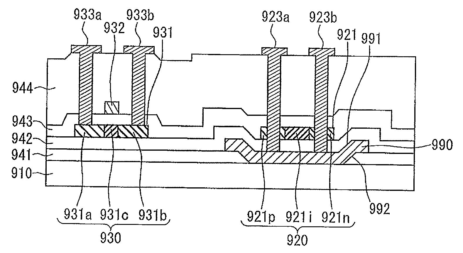
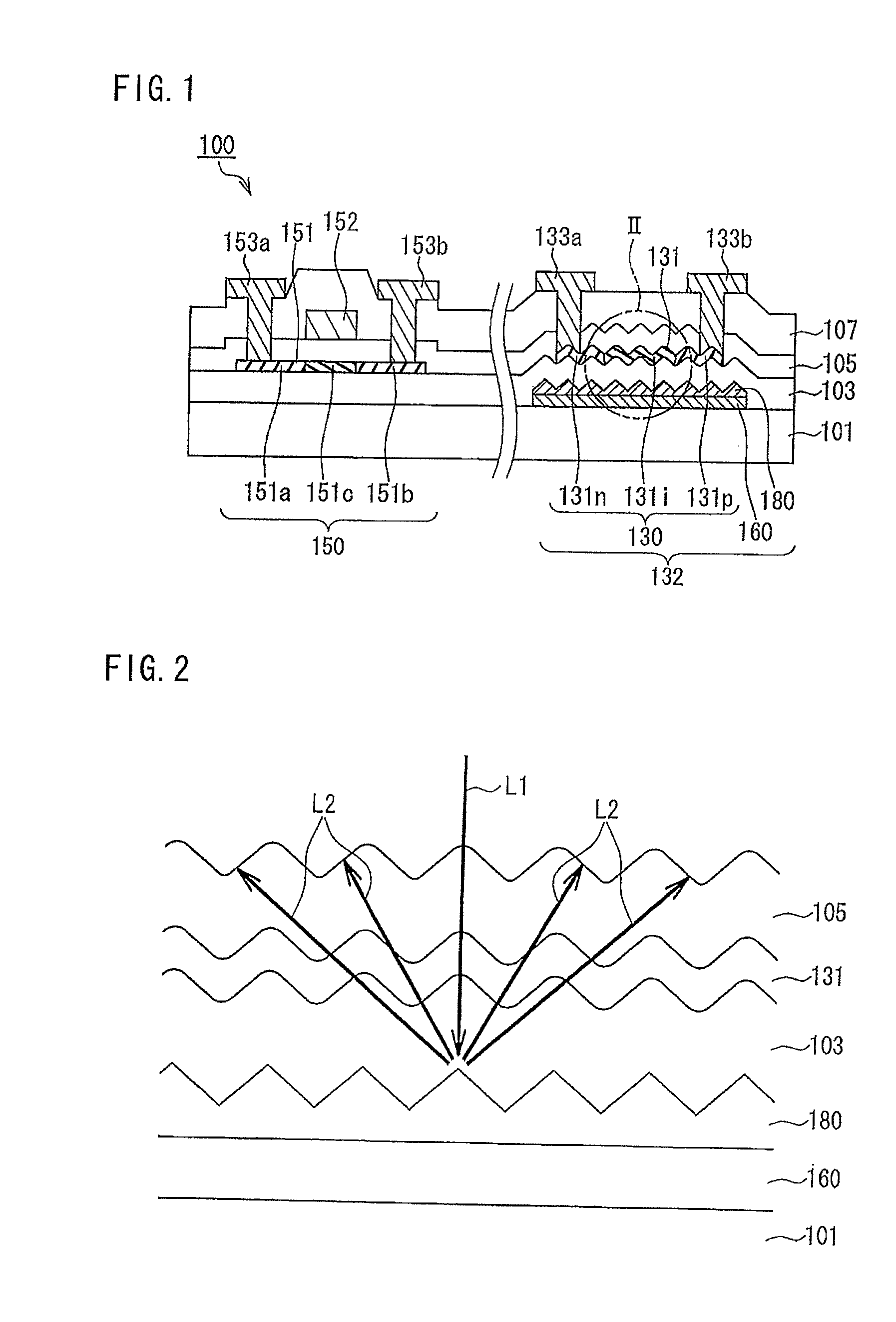
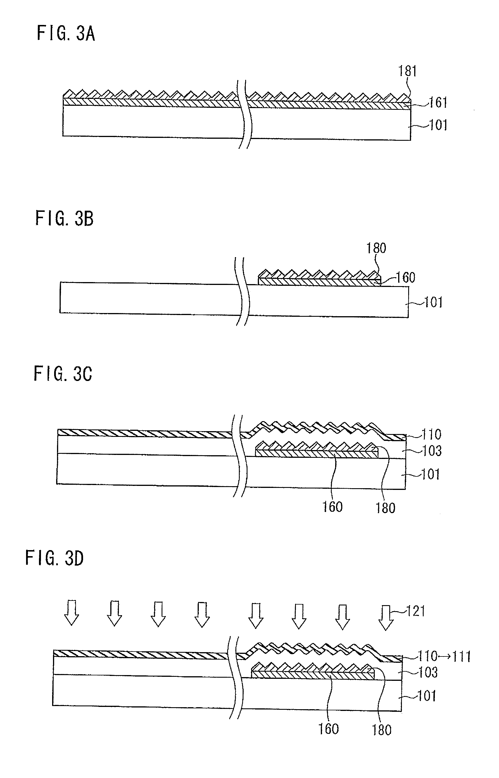
[0050]FIG. 1 is a schematic cross sectional view of a semiconductor device 100 according to Embodiment 1 of the present invention. The semiconductor device 100 includes: a photosensor 132 having a substrate 101, a thin film diode 130 formed above the substrate 101 with interposed base layer 103 therebetween as an insulating layer, and a light-blocking layer 160 provided between the substrate 101 and the thin film diode 130; and a thin film transistor 150. The substrate 101 is preferably translucent. To simplify the drawing, FIG. 1 only shows a single photosensor 132 and a single thin film transistor 150; however, a plurality of photosensors 132 and a plurality of thin film transistors 150 may be formed on a common substrate 101. Further, to facilitate understanding, FIG. 1 shows a cross section of the photosensor 132 and that of the thin film transistor 150 in the same drawing; however, these cross sections do not have to be on a single common plane.

[0051]The thin film diode 130 has...

embodiment 2

[0096]Embodiment 2 illustrates a liquid crystal panel including a semiconductor device having light detection functionality illustrated in Embodiment 1.

[0097]FIG. 4 is a schematic cross sectional view of a liquid crystal display device 500 including a liquid crystal panel 501 according to Embodiment 2.

[0098]The liquid crystal display device 500 includes a liquid crystal panel 501, an illuminating device 502 that illuminates the backside of the liquid crystal panel 501, and a translucent protection panel 504 disposed above the liquid crystal panel 501 with an air gap 503 interposed therebetween.

[0099]The liquid crystal panel 501 includes a TFT array substrate 510 and a counter substrate 520, both of which are translucent plates, and a liquid crystal layer 519 enclosed between the TFT array substrate 510 and the counter substrate 520. The TFT array substrate 510 and the counter substrate 520 are not limited to any particular material. The same materials that are used in conventional l...


PUM


Abstract

The light use efficiency of a thin film diode is improved even when the semiconductor layer of the diode has a small thickness, thereby improving the light detection sensitivity of the diode. Further, a short circuit between the electrodes of the thin film diode via the light-blocking layer is prevented. A thin film diode (130) having a first semiconductor layer (131) including, at least, an n-type region (131n) and a p-type region (131p) is provided on one side of a substrate (101), and a light-blocking layer (160) is provided between the substrate and the first semiconductor layer. A metal oxide layer (180) is provided on the side of the light-blocking layer facing the first semiconductor layer. Asperities are provided on the side of the metal oxide layer facing the first semiconductor layer, and the first semiconductor layer has a geometry of asperities conforming with the asperities on the metal oxide layer.

Description

REFERENCE TO RELATED APPLICATIONS[0001]This application is the national stage under 35 USC 371 of International Application No. PCT / JP2010 / 062552, filed Jul. 26, 2010, which claims priority of Japanese Patent Application No. 2009-190982, filed Aug. 20, 2009, the entire contents of which are incorporated herein by reference.FIELD OF THE INVENTION[0002]The present invention relates to a photosensor that includes a thin film diode (TFD) having a semiconductor layer including, at least, an n-type region and a p-type region. Further, the present invention relates to a semiconductor device including a thin film diode and a thin film transistor (TFT). Furthermore, the present invention relates to a liquid crystal panel including such a semiconductor device.BACKGROUND OF THE INVENTION[0003]Touch sensor functionality can be established by incorporating a photosensor including a thin film diode into a display device. In such a display device, information can be input as a finger or a touch pe...

Claims


Application Information

Patent Timeline
IPC IPC(8): H01L29/786
CPCH01L27/1214H01L31/101H01L31/02164H01L27/14601
Inventor ODA, AKIHIROKANEKO, SEIJI
Owner SHARP KK
Why Eureka
Try Eureka