High performance organic transistor photodetector based on bulk heterojunction-layered structure

A photodetector, organic transistor technology, applied in photovoltaic power generation, semiconductor devices, electro-solid devices, etc., can solve the problems of OPTs photocurrent drop, inability to achieve efficient transport, hole transport obstacles, etc., to improve light detection. Sensitivity, reduce the probability of recombination, and ensure the effect of efficient transmission

Active Publication Date: 2021-07-30
SHENZHEN INST OF ADVANCED TECH
View PDF7 Cites 0 Cited by
  • Summary
  • Abstract
  • Description
  • Claims
  • Application Information

AI Technical Summary

Problems solved by technology

However, since there are also quantum dots or polymers in the channels of OPTs, these quantum dots or polymers themselves will become obstacles to hole transport when holes are transported in the channels.
Holes are transported in the organic semiconductor through hopping mode. When there are quantum dots in the channel, these quantum dots are essentially n-type semiconductors, which is equivalent to creating a large potential barrier for the holes, and the holes will be scattered and hindered, thus High-efficiency transport cannot be achieved, which will directly lead to a decrease in the photocurrent of OPTs and a prolonged response time (the time response is related to the mobility of channel carriers)

Method used


Image

  • High performance organic transistor photodetector based on bulk heterojunction-layered structure
  • High performance organic transistor photodetector based on bulk heterojunction-layered structure
  • High performance organic transistor photodetector based on bulk heterojunction-layered structure

Examples


preparation example Construction

[0048] The present invention also provides a method for preparing a high-performance organic transistor photodetector, comprising the following steps:

[0049] 1) Prepare the gate and gate dielectric layers sequentially on the substrate, place the substrate in acetone, isopropanol or ethanol, and deionized water in order to ultrasonically clean the substrate for 10 minutes, and clean the substrate with N 2 gun dry;

[0050] 2) Subject the substrate to UV / ozone or O 2 plasma treatment;

[0051] 3) Perform surface monomolecular layer self-assembly processing on the gate dielectric layer to generate a monomolecular self-assembly layer;

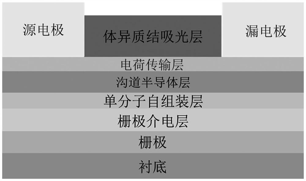
[0052] 4) Depositing a channel semiconductor layer on the monomolecular self-assembled layer;

[0053] 5) forming a charge transport layer on the channel semiconductor layer;

[0054] 6) Vacuum-evaporating a source electrode and a drain electrode on both sides of the charge transport layer, wherein a channel region is formed between the sourc...
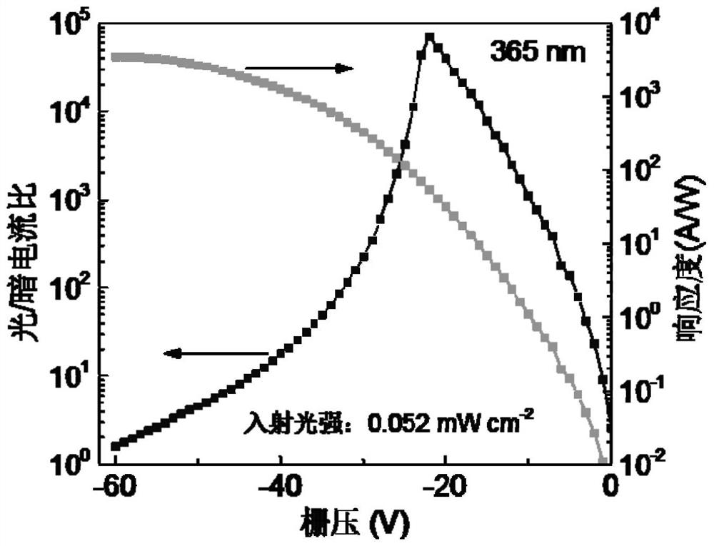
Embodiment 1

[0057] This embodiment is used to illustrate the high-performance organic transistor ultraviolet photodetector provided by the present invention and its preparation method.

[0058] In this embodiment, a silicon wafer is used as the substrate, C8-BTBT is used as the organic semiconductor material, and MoO 3 As a charge transport layer, PC 61 BM is used as the charge acceptor material, Au is used as the source and drain electrodes, and the photodetector prepared is an ultraviolet photodetector. The silicon wafer used is heavily doped p-type Si as the gate and a layer of thermally oxidized SiO with a thickness of 200nm on the surface 2 as a gate dielectric.

[0059] A method for preparing a high-performance organic transistor ultraviolet photodetector based on a bulk heterojunction-layered structure, comprising the following steps:

[0060] (1) Place the silicon substrate successively in acetone, isopropanol, and deionized water for 10 min, and use N 2 The gun is blown dry, ...
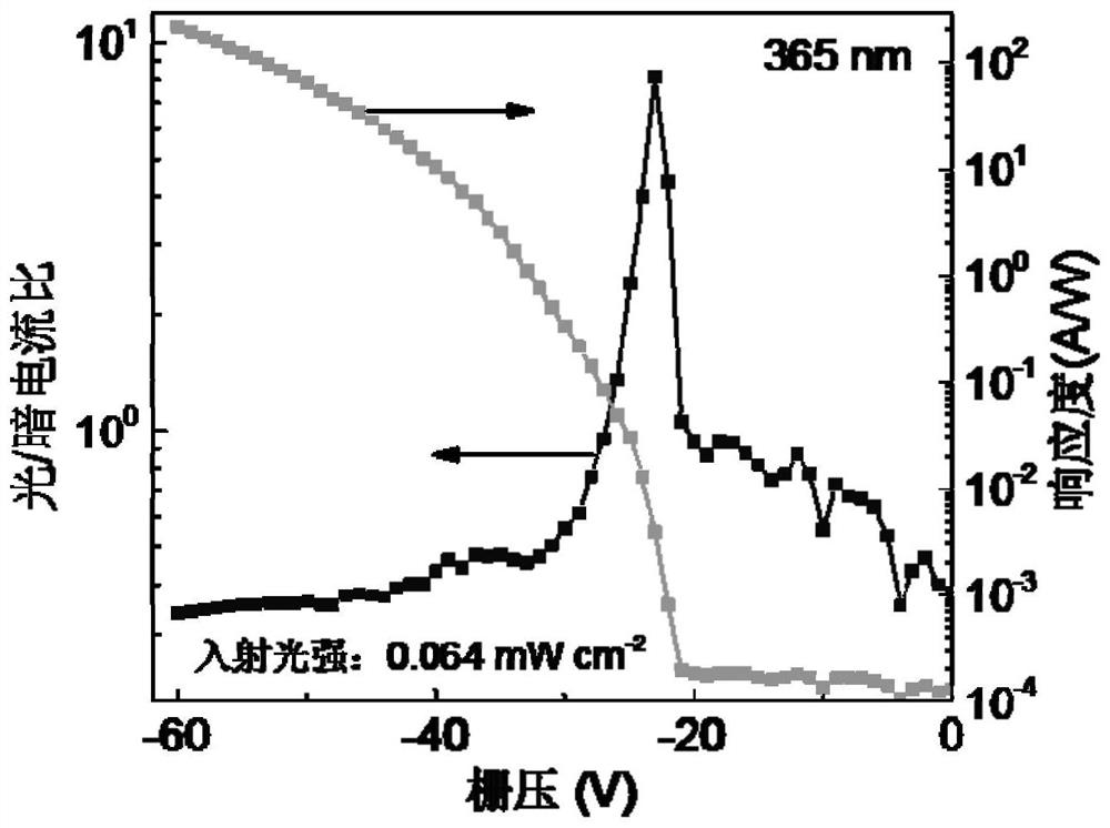
Embodiment 2

[0079] This embodiment is used to illustrate the high-performance organic transistor ultraviolet photodetector provided by the present invention and its preparation method.

[0080] In this embodiment, a silicon wafer is used as the substrate, C8-BTBT is used as the organic semiconductor material, and MoO3 As a charge transport layer, PC 61 BM is used as the charge acceptor material, Au is used as the source and drain electrodes, and the photodetector prepared is an ultraviolet photodetector. The silicon wafer used is heavily doped p-type Si as the gate and a layer of thermally oxidized SiO with a thickness of 200nm on the surface 2 as a gate dielectric.

[0081] A method for preparing a high-performance organic transistor ultraviolet photodetector based on a bulk heterojunction-layered structure, comprising the following steps:

[0082] (1) Place the silicon substrate successively in acetone, isopropanol, and deionized water for 10 min, and use N 2 The gun is blown dry, an...


PUM

PropertyMeasurementUnit
thicknessaaaaaaaaaa
lengthaaaaaaaaaa
widthaaaaaaaaaa

Abstract

The invention discloses a high-performance organic transistor photodetector based on a bulk heterojunction-layered structure, including a substrate and a gate, a gate dielectric layer, a single-molecule self-assembly layer, A channel semiconductor layer and a charge transport layer, a source electrode and a drain electrode are also provided on a part of the charge transport layer, and a bulk heterogeneous electrode is also provided in the channel region between the source electrode and the drain electrode on the charge transport layer. Matte light-absorbing layer. The organic transistor photodetector of the present invention is based on the above-mentioned specific layered structure, can make full use of the CTE effect, effectively separate the photogenerated excitons and reduce their recombination probability, ensure the efficient transmission of charge carriers in the channel, and significantly improve the performance of OPTs devices. Light detection sensitivity and other comprehensive performance.

Description

technical field [0001] The invention belongs to the field of semiconductor optoelectronic devices, and in particular relates to a high-performance organic transistor based on a bulk heterojunction-layered structure and a photodetector comprising the organic transistor, and more particularly relates to a working band of ultraviolet light, Visible light, infrared light and full-band high-performance organic transistors based on bulk heterojunction-layered structure. Background technique [0002] A photodetector is a device that converts optical signals into electrical signals, and has important applications in various fields of military and national economy. Before the 1980s, photodetectors were mainly based on inorganic semiconductors, such as GaN and SiC, whose preparation process was complicated and costly. In comparison, organic phototransistors (OPTs) with organic field-effect transistors (Organic Field-effect Transistors, OFETs) as functional devices have high sensitivi...

Claims


Application Information

Patent Timeline
Patent Type & Authority Patents(China)
IPC IPC(8): H01L51/42H01L51/48
CPCH10K30/65H10K30/354H10K30/30Y02E10/549
Inventor 李佳高源鸿易亚喻学锋
Owner SHENZHEN INST OF ADVANCED TECH
Why Eureka
Try Eureka