

Method of fabricating an integrated circuit having a strain inducing hollow trench isolation region
- Summary
- Abstract
- Description
- Claims
- Application Information
AI Technical Summary
Benefits of technology
Problems solved by technology
Method used
Image

Examples
Embodiment Construction
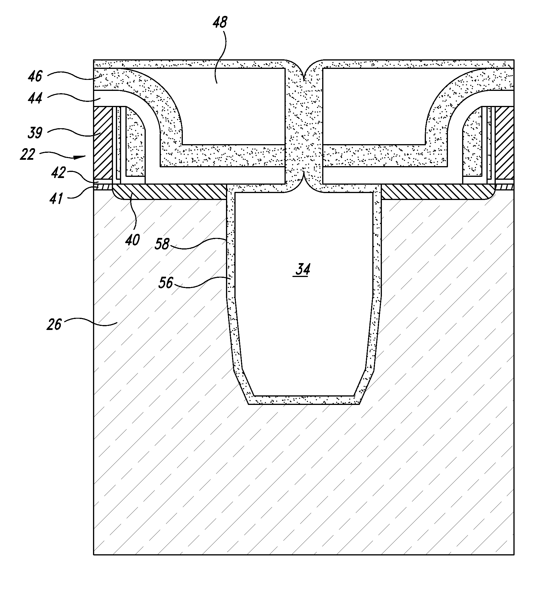
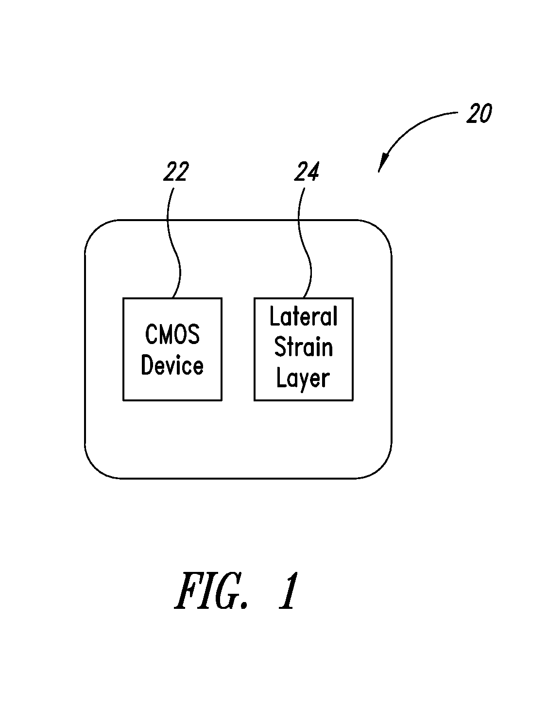
[0026]FIG. 1 is a block diagram of an integrated circuit according to one embodiment of the invention. The integrated circuit 20 comprises a CMOS device 22 and a lateral strain layer 24 adjacent the CMOS device 22. The lateral strain layer 24 induces a strain on the CMOS device 22 and improves device characteristics.
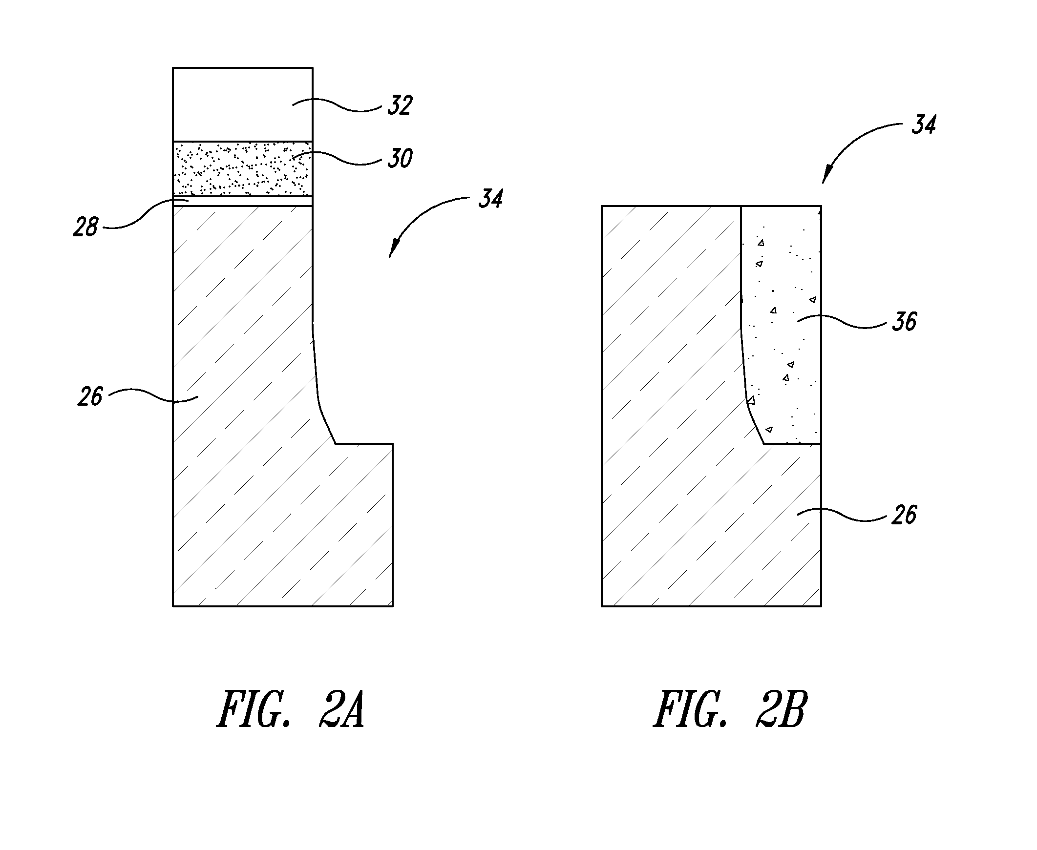
[0027]Biaxial strain can be induced in the channel region of a transistor by forming a lattice junction between two dissimilar materials. One example of a lattice junction between two dissimilar materials is where a layer of monocrystalline Si joins a layer of SiGe. The crystal structures of the two materials join at the interface. In the case of SiGe and Si the spacing between atoms in a SiGe crystal structure is larger than the spacing between atoms in a Si crystal structure, but the difference is small enough that the two lattices can bond. At the interface of SiGe and Si, the larger lattice spacing of the SiGe causes a biaxial tensile strain in the atoms of the Si la...
PUM
 Abstract
Description
Claims
Application Information