Electrochromic device

a technology of electrochromic devices and electrodes, applied in the field of electrochromic devices, can solve the problems of not working properly on large-area displays or electrochromic devices, and not appropriately solving the above problems

Inactive Publication Date: 2012-06-14
APPLIED NANOTECH HLDG
View PDF8 Cites 39 Cited by
  • Summary
  • Abstract
  • Description
  • Claims
  • Application Information

AI Technical Summary

Problems solved by technology

Systems have been developed in the past that do not appropriately solve the above problems.
A drawback with these films is that they do not properly work on large area displays or electrochromic devices, having square meter surfaces.

Method used


Image

  • Electrochromic device
  • Electrochromic device
  • Electrochromic device

Examples


Embodiment Construction

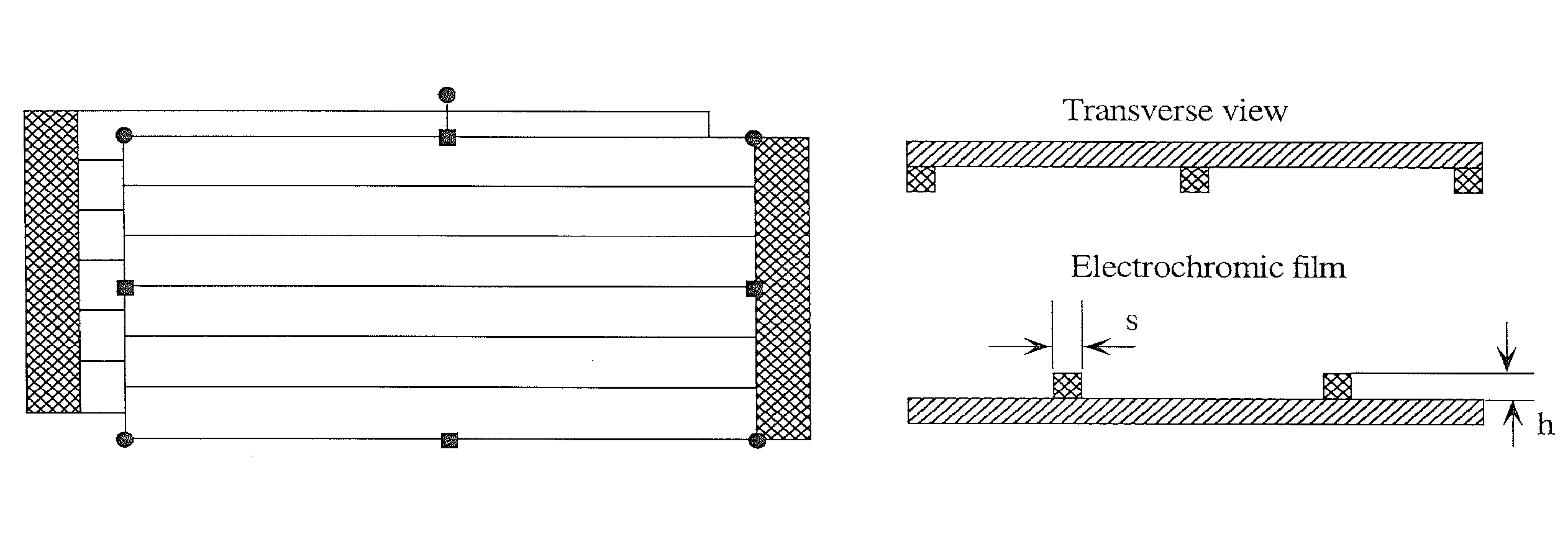
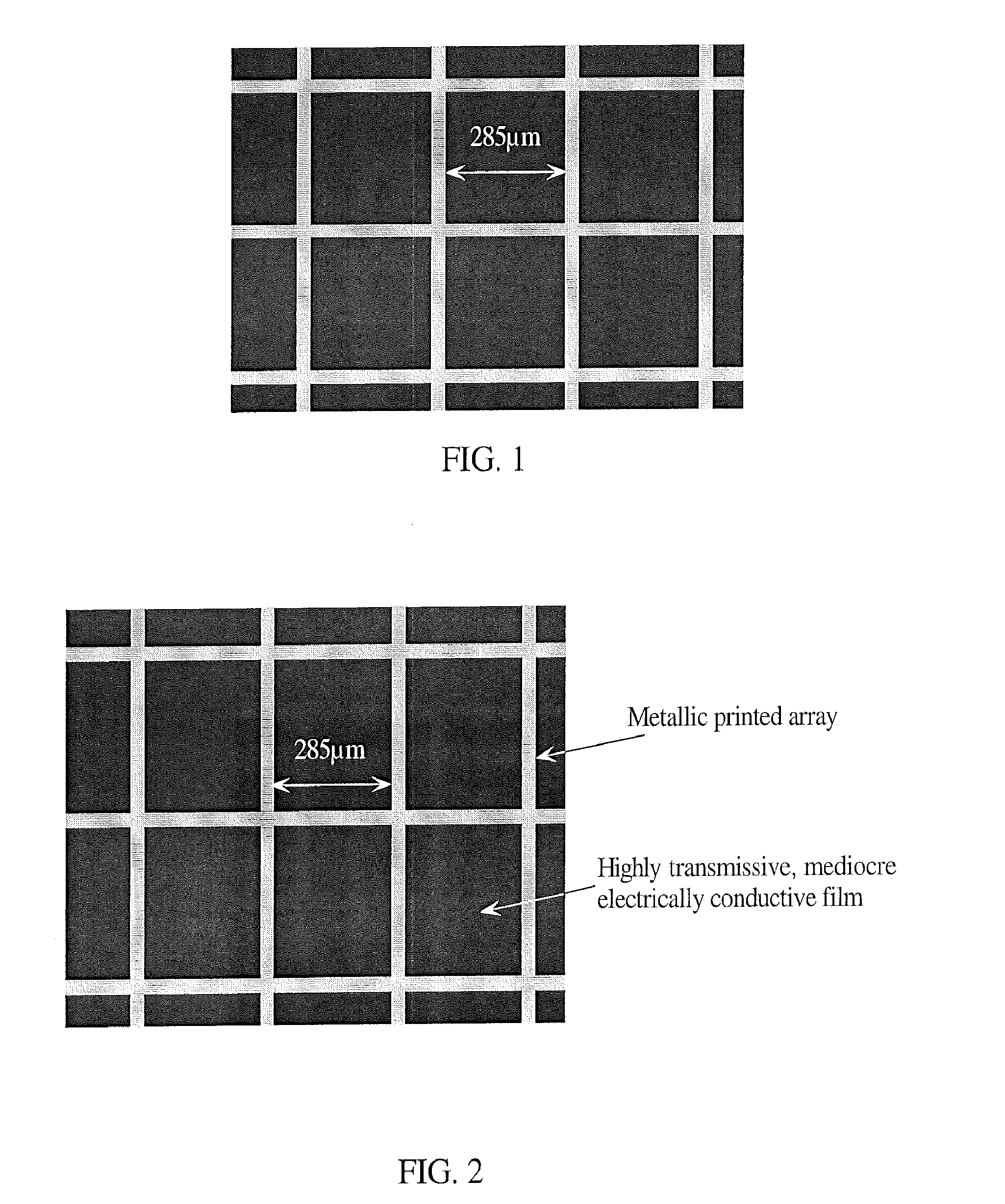
[0021]FIG. 1 illustrates a solution to the aforementioned problems that utilizes films with an array of metal wires deposited or printed on the optically transmissive substrate, utilizing very conductive metals such as Ag, Cu, etc. By doing so at variable resolutions and densities, one can achieve suitable optical transmission, on one hand, and also resistivity as low as 10−3 ohm / sq or lower. These conductive supports can be produced by low cost processes, for example through an inkjet process or any other process like screen printing to deposit copper ink followed by photosintering, as described in U.S. Patent Application Ser. Nos. 61 / 053,574 and 61 / 081,539, which are incorporated by reference herein.

[0022]A problem is that in many of the applications, such as display and electrochromic windows, it is necessary to apply the electric field continuously, meaning that there are not any locations on the substrate where no conductive electrode is available. Referring to FIG. 2, printing...


PUM

PropertyMeasurementUnit
transparentaaaaaaaaaa
thicknessaaaaaaaaaa

Abstract

A method for manufacturing an electrochromic window positions a pattern of conductive lines over a first transparent substrate, a transparent conductive film over the pattern of conductive lines and first transparent substrate, and an electrochromic layer over the transparent conductive film, wherein the transparent conductive layer is a physical barrier separating the electrochromic layer from the pattern of conductive lines. The first transparent substrate may be flexible. The pattern of conductive lines and transparent conductive film may be deposited and processed at a temperature less than 180 degrees C. The pattern of conductive lines may be deposited on the first transparent substrate by printing techniques.

Description

[0001]This application claims priority to U.S. Provisional Application Ser. Nos. 61 / 233,371 and 61 / 151,423, which are hereby incorporated by reference herein.BACKGROUND INFORMATION[0002]In the flexible electronic industry, flexible displays, electrochromic windows, and solar cells, etc. need highly optically transmissive properties in the visible range as well as having a highly electrically conductive surface. For example, for the expensive active matrix LCD industry, high quality ITO films are deposited at relatively high temperatures by spattering or evaporation techniques in order to achieve high optical transmissivity and electrical resistivity not larger than 10 ohm / sq, and more preferably 1 ohm / sq (“ohm / sq” is a common unit for “ohms per square,” which is dimensionally equal to an ohm, but is used for sheet resistance). As these applications increase in size, the problem of electrical conductivity becomes more critical in achieving optical uniformity and functionality over th...

Claims


Application Information

Patent Timeline
Patent Type & Authority Applications(United States)
IPC IPC(8): G02F1/161H05K3/02
CPCY10T29/49155G02F1/155
Inventor YANIV, ZVICHIDICHIMO, GIUSEPPEDE SIMONE, BRUNA CLARAIMBARDELLI, DANIELA
Owner APPLIED NANOTECH HLDG
Why Eureka
Try Eureka