Image sensor having supplemental capacitive coupling node

a capacitive coupling node and image sensor technology, applied in the field of image sensors, can solve the problems of pixel saturation or overexposure in bright environments, and achieve the effect of increasing the intensity of pixel saturation or overexposur

Active Publication Date: 2012-06-21
OMNIVISION TECH INC
View PDF5 Cites 50 Cited by
  • Summary
  • Abstract
  • Description
  • Claims
  • Application Information

AI Technical Summary

Problems solved by technology

However, as pixel cell sizes continue to shrink, pixel saturation or overexposure in bright environments is becoming more acute.

Method used


Image

  • Image sensor having supplemental capacitive coupling node
  • Image sensor having supplemental capacitive coupling node
  • Image sensor having supplemental capacitive coupling node

Examples


Embodiment Construction

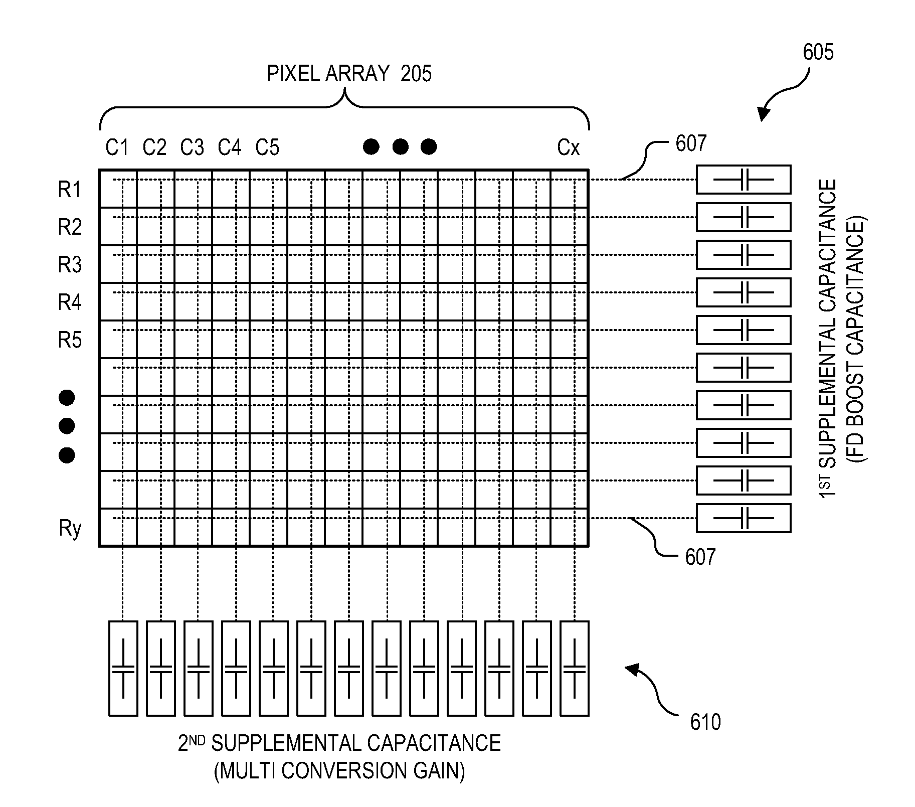
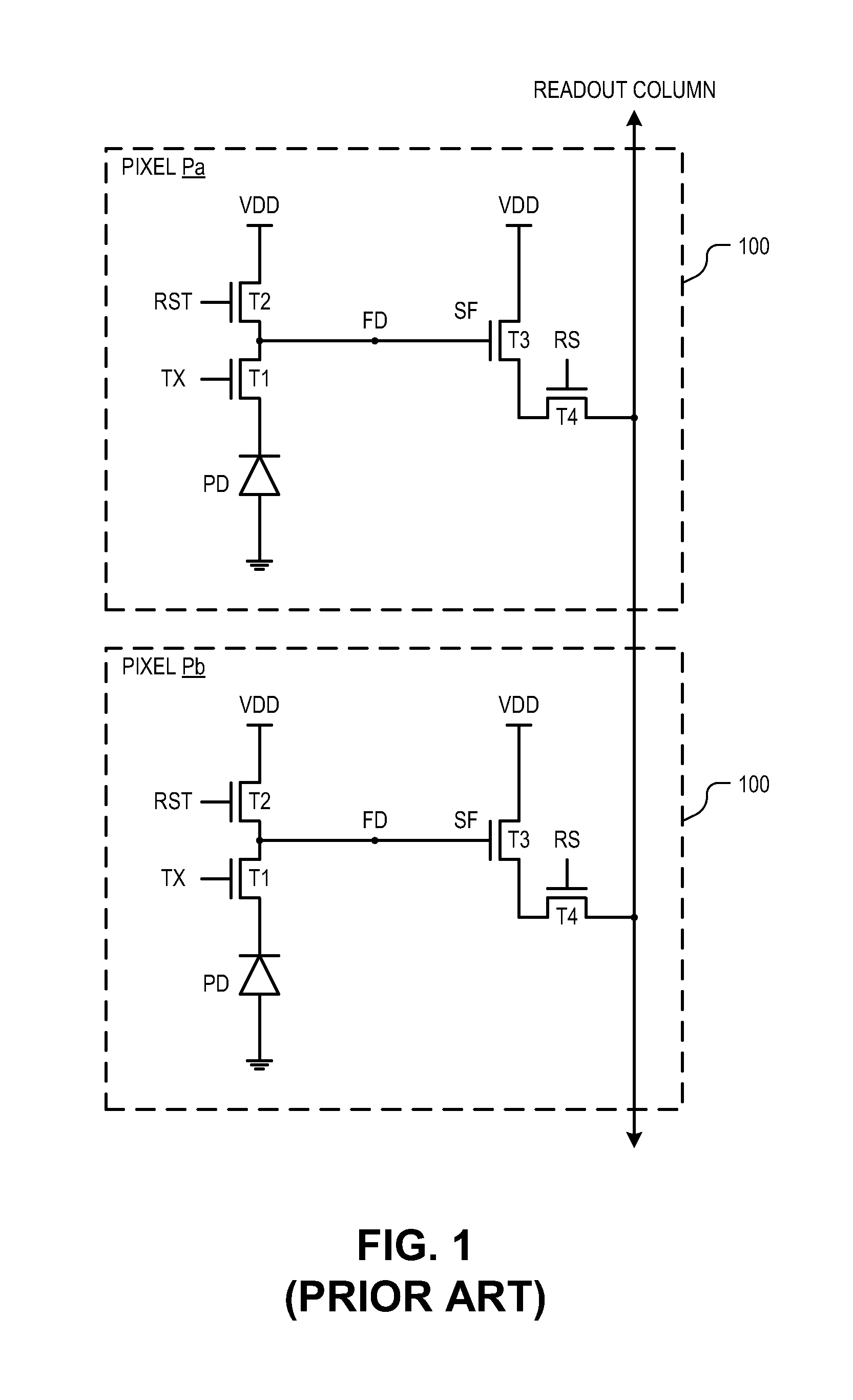
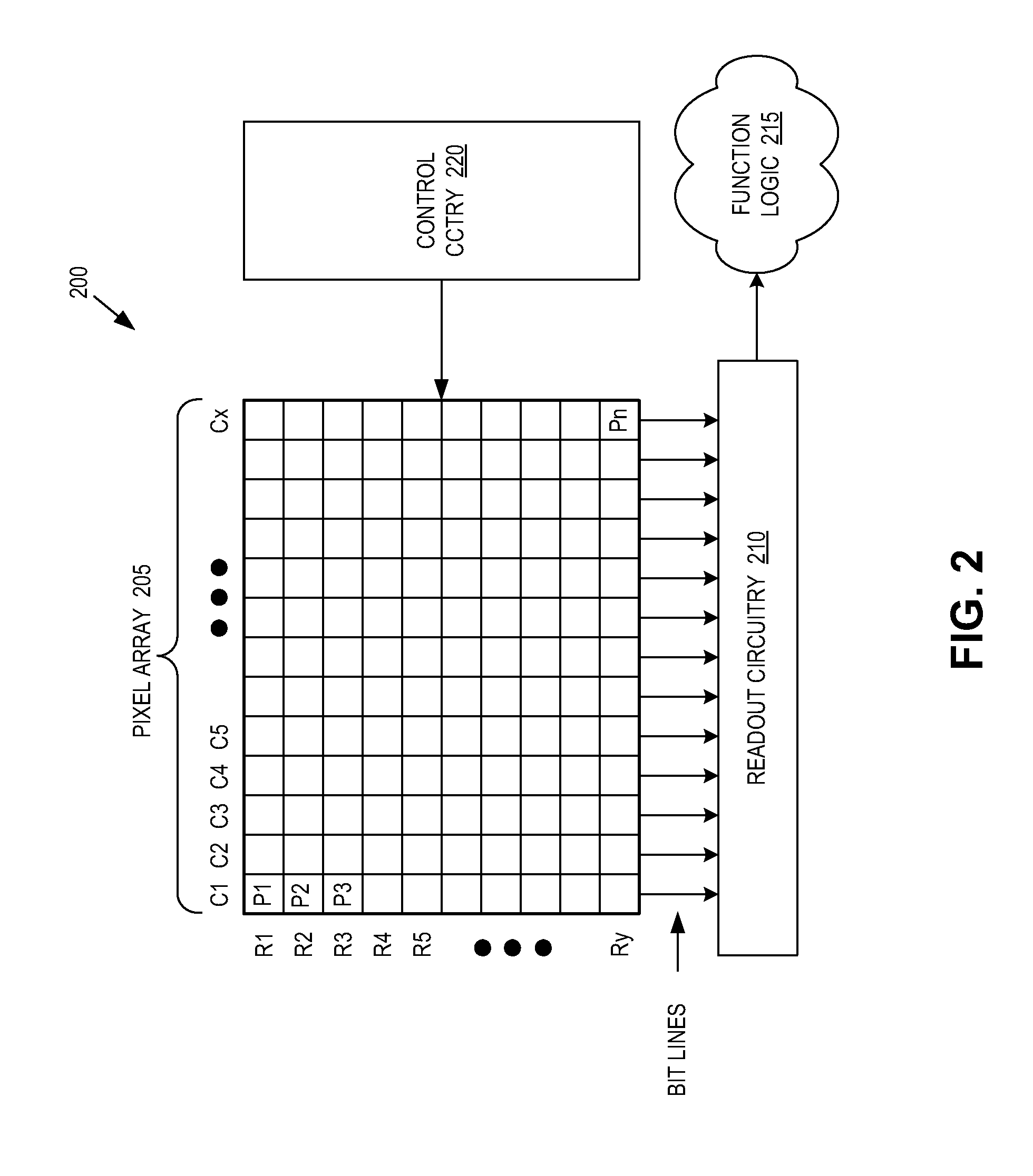
[0020]Embodiments of a CMOS image sensor including a supplemental capacitive coupling node are described herein. In the following description, numerous specific details are described to provide a thorough understanding of embodiments of the invention. One skilled in the relevant art will recognize, however, that the invention can be practice without one or more of the specific details, or with other methods, components, materials, etc. In other instances, well-known structures, materials or operations are not shown or described in details but are nonetheless encompassed within the scope of the invention.

[0021]Reference throughout this specification to “one embodiment” or “an embodiment” means that a particular feature, structure, or characteristic described in connection with the embodiment is included in at least one embodiment of the present invention. Thus, the appearances of the phrases “in one embodiment” or “in an embodiment” in various places throughout this specification are...


PUM


Abstract

An image sensor includes a pixel array, a bit line, supplemental capacitance node line, and a supplemental capacitance circuit. The pixel array includes a plurality of pixel cells each including a floating diffusion (“FD”) node and a photosensitive element coupled to selectively transfer image charge to the FD node. The bit line is coupled to selectively conduct image data output from a first group of the pixel cells. The supplemental capacitance node line is coupled to the FD node of a second group of the pixel cells to selectively couple a supplemental capacitance to the FD nodes of the second group in response to a control signal. In various embodiments, the first and second group of pixel cells may be the same group or a different group of the pixel cells and may add a capacitive boost feature or a multi conversion gain feature.

Description

TECHNICAL FIELD[0001]This disclosure relates generally to image sensors, and in particular, but not exclusively to complementary metal-oxide semiconductor (“CMOS”) image sensors.BACKGROUND INFORMATION[0002]Image sensors have become ubiquitous. They are widely used in digital still cameras, cellular phones, security cameras, as well as, medical, automobile, and other applications. The technology used to manufacture image sensors, and in particular, complementary metal-oxide-semiconductor (“CMOS”) image sensors (“CIS”), has continued to advance at great pace. For example, the demands of higher resolution and lower power consumption have encouraged the further miniaturization and integration of these image sensors.[0003]FIG. 1 is a circuit diagram illustrating pixel circuitry of two four-transistor (“4T”) pixel cells Pa and Pb (collectively pixel cells 100) within an image sensor array. Pixel cells Pa and Pb are arranged in two rows and one column and time share a single readout column...

Claims


Application Information

Patent Timeline
Patent Type & Authority Applications(United States)
IPC IPC(8): H01L27/146
CPCH04N5/35509H04N5/3559H04N5/376H04N5/3597H04N5/37452H04N25/571H04N25/59H04N25/626H04N25/74H04N25/771
Inventor MAO, DULITAI, HSIN-CHIHVENEZIA, VINCENTRHODES, HOWARD E.MANABE, SOHEI
Owner OMNIVISION TECH INC
Why Eureka
Try Eureka