Channel-etch type thin film transistor and method of manufacturing the same

Inactive Publication Date: 2012-06-21
CANON KK
View PDF2 Cites 26 Cited by
  • Summary
  • Abstract
  • Description
  • Claims
  • Application Information

AI Technical Summary

Benefits of technology

[0013]Thus, a channel-etch type TFT using an oxide semiconductor for the channel layer thereof according to the present invention represents an improved uniformity in terms of film thickness of the channel layer after wet etching as well as TFT characteristics with an improved uniformity thereof. When an oxide semiconductor containing In, Ga and Zn like the sacrificial layer is used for the channel layer (i.e. with the same component elements and the same composition as those of the sacrificial layer), the channel layer and the sacrificial layer can be formed successively by means of the same apparatus to achieve a high manufacturin

Problems solved by technology

Furthermore, the low resistivity of the sacrificial layer by turn reduces the

Method used


Image

  • Channel-etch type thin film transistor and method of manufacturing the same
  • Channel-etch type thin film transistor and method of manufacturing the same
  • Channel-etch type thin film transistor and method of manufacturing the same

Examples


example 1

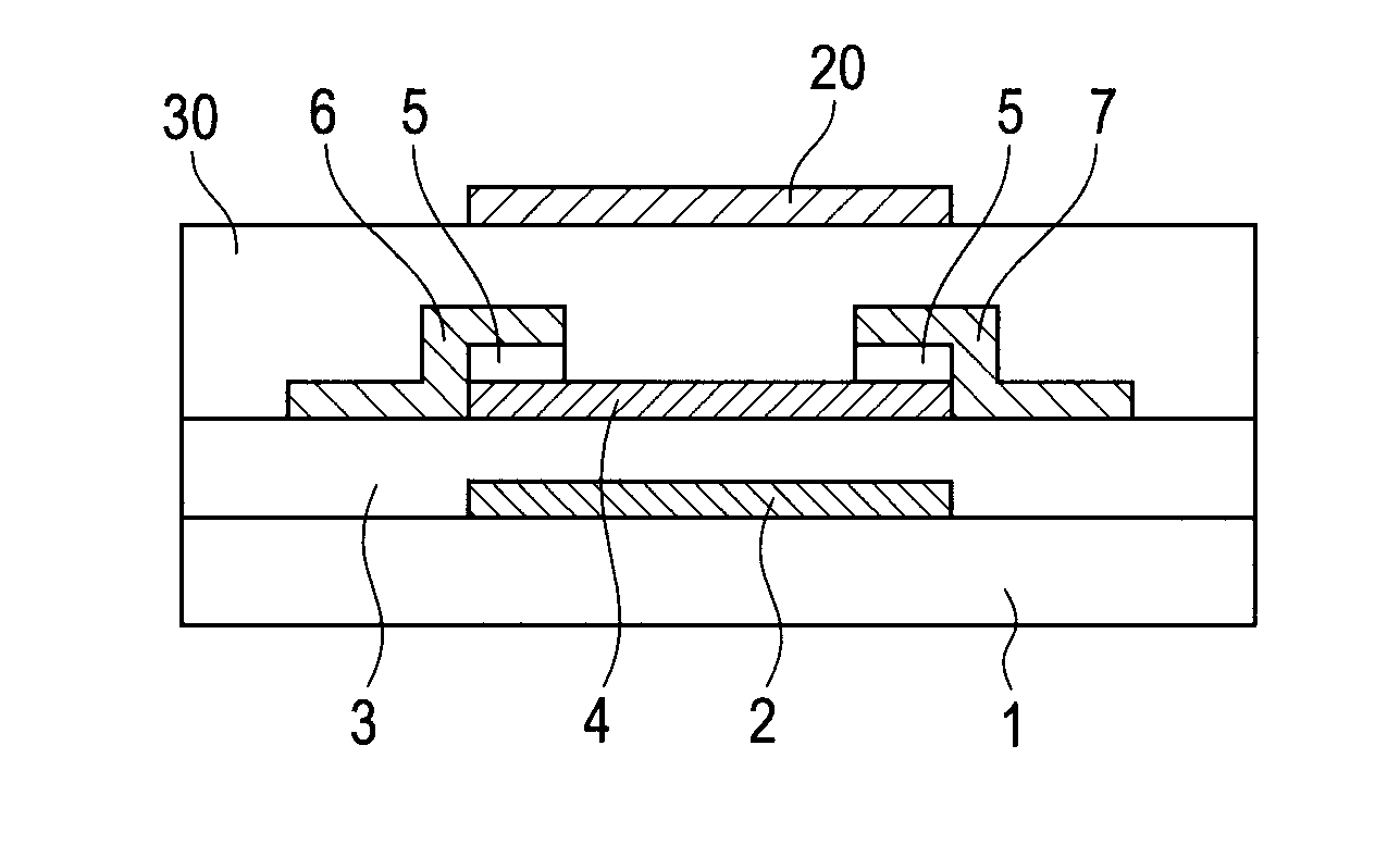
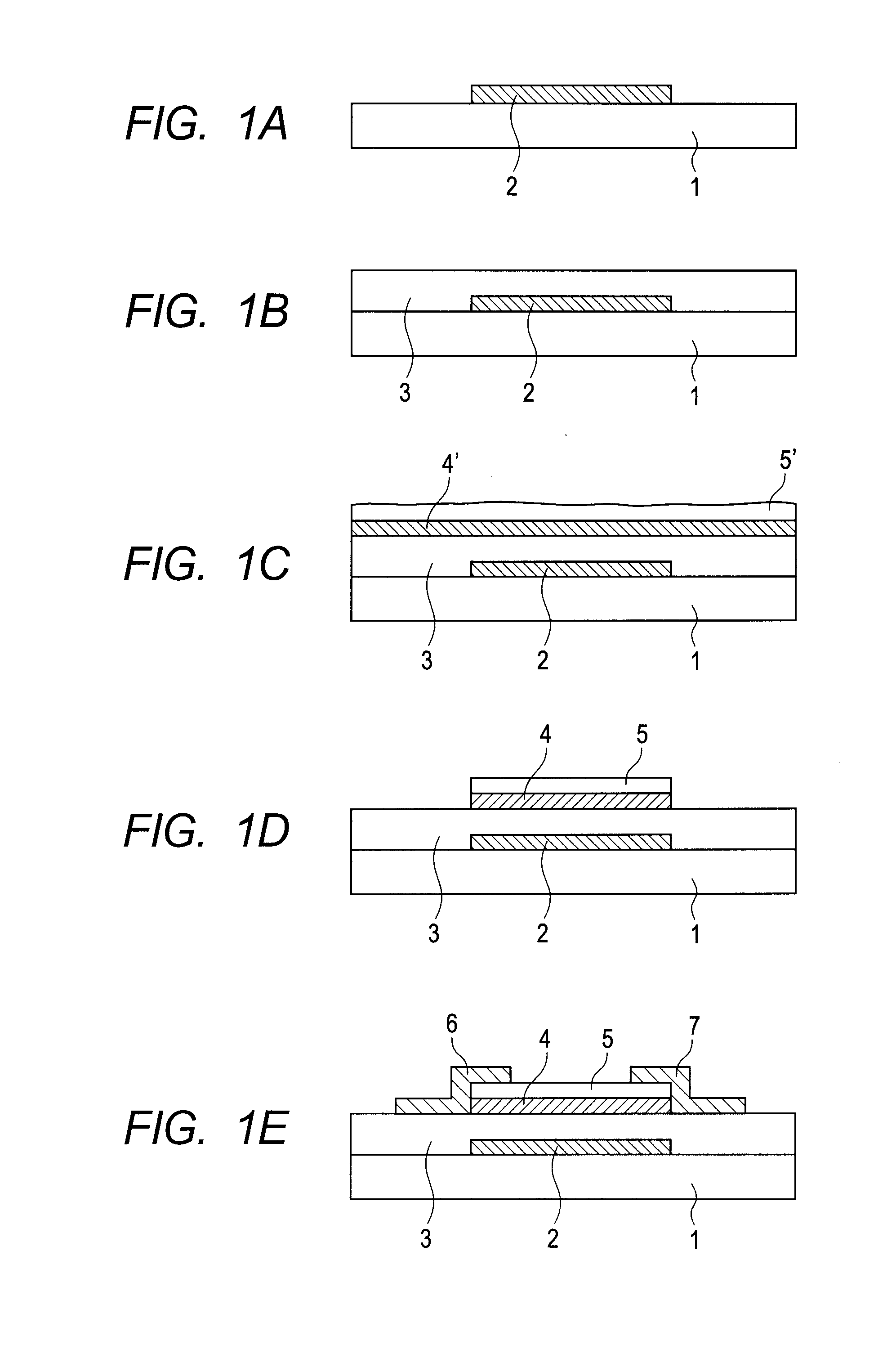
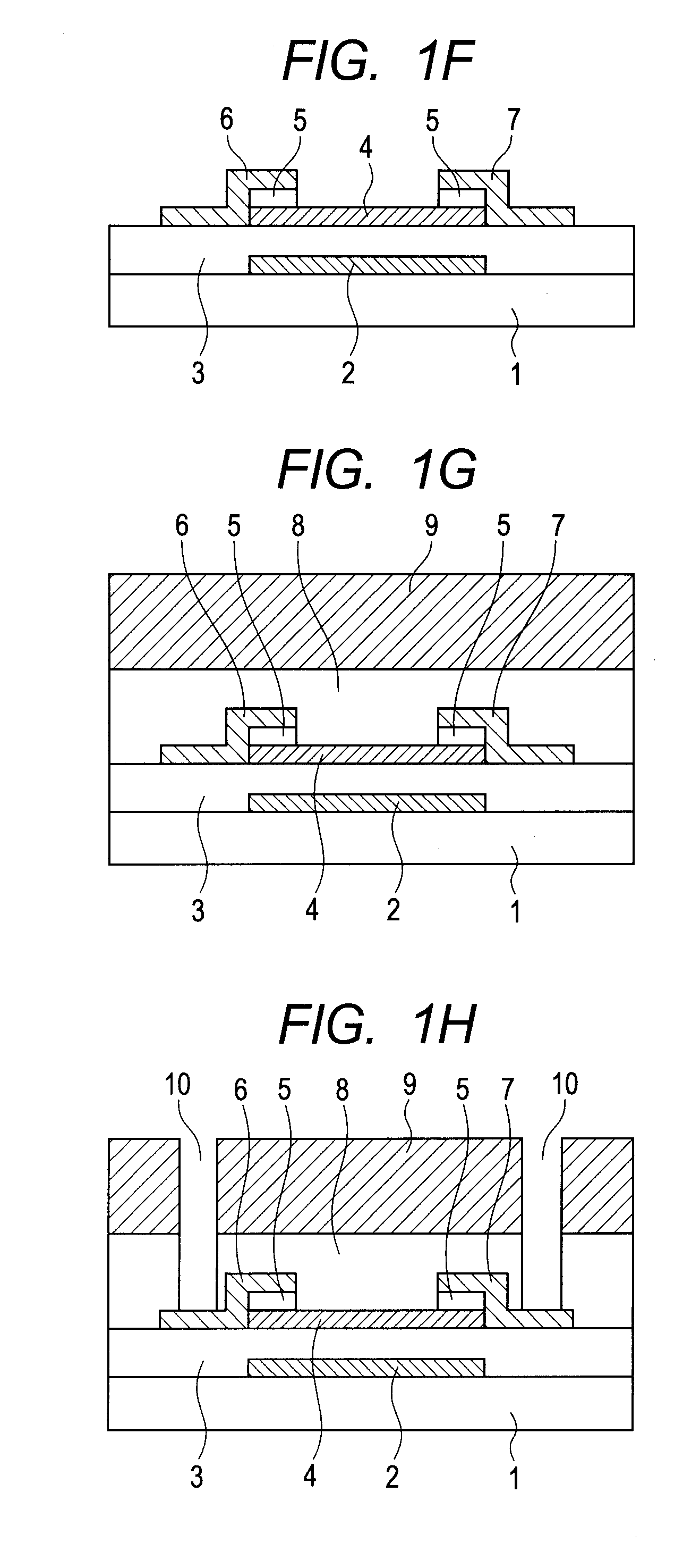
[0053]A bottom gate, channel-etch type TFT was prepared by following the steps illustrated in FIGS. 1A through 1H. Now, each of the steps will be described below.

[0054]A glass substrate (1737, available from Corning) was used for the substrate 1. The glass substrate had a thickness of 0.5 mm. Firstly a 100 nm-thick Mo thin film was formed on the substrate 1 by means of DC magnetron sputtering in an atmosphere of Ar gas. Then, the deposited Mo thin film was micro-processed to produce a gate electrode 2 by means of photolithography and dry etching (FIG. 1A).

[0055]Thereafter, a 200 nm-thick SiO2 thin film was formed as a gate insulating layer 3 on the gate electrode 2 by plasma CVD (FIG. 1B).

[0056]Subsequently, a 40 nm-thick In—Ga—Zn—O thin film (oxide semiconductor layer 4′) was formed on the gate insulating layer 3 by means of DC magnetron sputtering with a DC power supply rate of 3.7 W / cm2. The In—Ga—Zn—O thin film formed in this way was amorphous and the composition ratio of In:Ga:...


PUM


Abstract

A channel layer is formed on a substrate by using an oxide semiconductor and then a sacrificial layer of an oxide containing In, Zn and Ga and representing an etching rate greater than the etching rate of the oxide semiconductor is formed on the channel layer. Thereafter, a source electrode and a drain electrode are formed on the sacrificial layer and the sacrificial layer exposed between the source electrode and the drain electrode is removed by means of wet etching.

Description

BACKGROUND OF THE INVENTION[0001]1. Field of the Invention[0002]The present invention relates to a channel-etch type thin film transistor using an oxide semiconductor and a method of manufacturing the same. More particularly, the present invention relates to a thin film transistor having a structure formed by removing part of the channel layer that is damaged by dry etching for forming a drain electrode and a source electrode and a method of manufacturing such a thin film transistor.[0003]2. Related Background Art[0004]Liquid crystal displays and organic EL displays using thin film transistors (TFTs) as drive elements have been put into practical use in recent years. While amorphous Si and polycrystalline Si are mainly employed for semiconductor layers of such TFTs, researches are intensively being made on semiconductor materials other than Si. Instances of using amorphous oxides containing In, Ga and Zn (In—Ga—Zn—O) for semiconductor layers of TFTs have been reported recently. Such...

Claims


Application Information

Patent Timeline
IPC IPC(8): H01L29/786H01L21/34
CPCH01L29/78618H01L29/66969H01L29/7869H01L29/45H01L29/66742
Inventor YAGINUMA, SEIICHIROIWASAKI, TATSUYAHAYASHI, RYOKUMOMI, HIDEYAWATANABE, MASAYA
Owner CANON KK
Why Eureka
Try Eureka