

Insulated gate bipolar transistor and manufacturing method thereof
a technology of bipolar transistors and manufacturing methods, which is applied in the direction of transistors, electrical devices, semiconductor devices, etc., can solve the problems of poor power conversion efficiency, thermal breakage, and rise of transistors, and achieve the effect of reducing on-state voltag
- Summary
- Abstract
- Description
- Claims
- Application Information
AI Technical Summary
Benefits of technology
Problems solved by technology
Method used
Image

Examples
first preferred embodiment
Structure
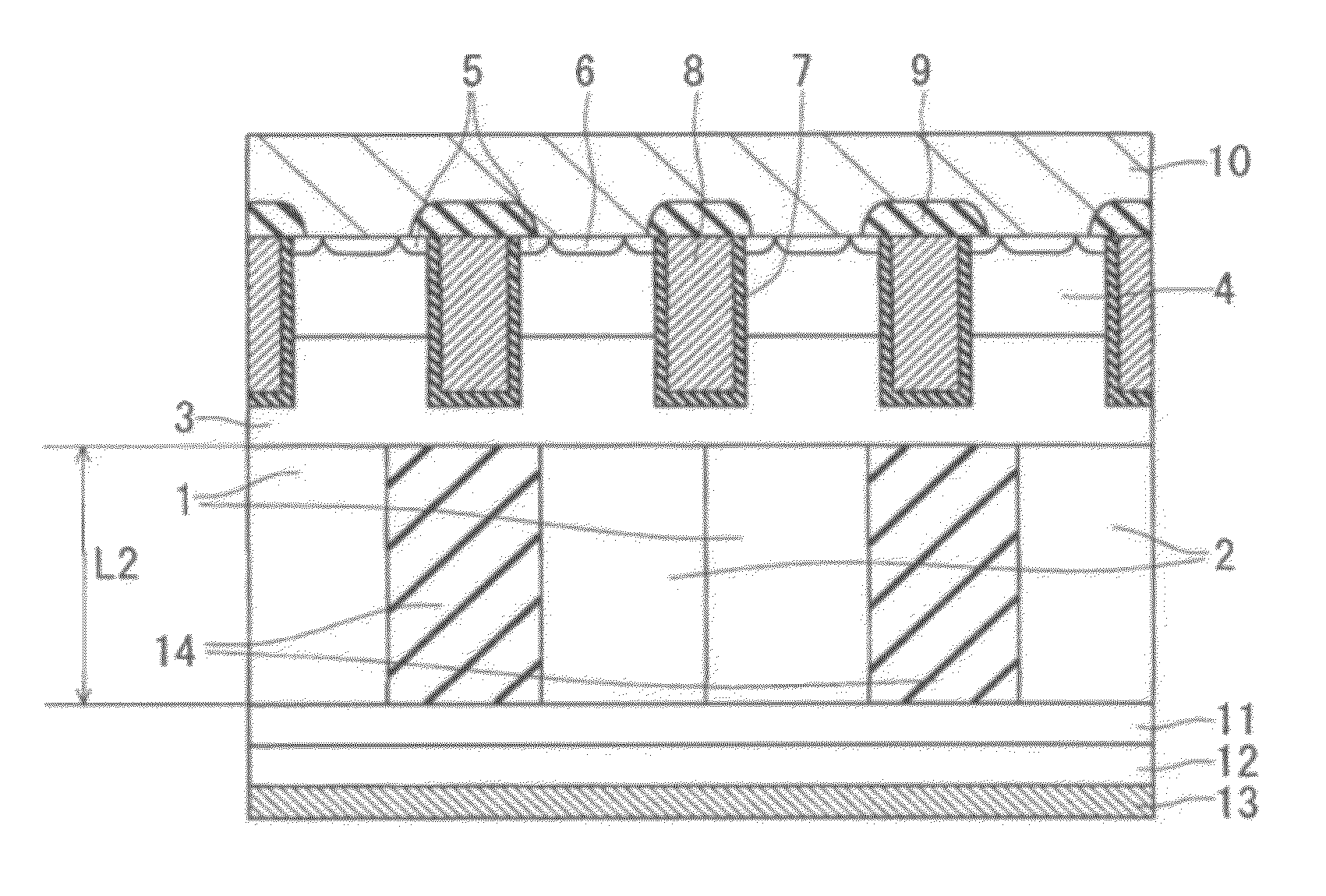
[0043]FIG. 1 is a cross-sectional view of a trench gate IGBT according to a first preferred embodiment.
[0044]In the IGBT of this preferred embodiment, a drift layer is formed over a P collector layer 12 with an N buffer layer 11 therebetween. The drift layer has a two-layered structure of a first drift layer and an N-drift layer 3 as a second drift layer. The first drift layer has a super junction structure in which an N-drift layer 1 as a first layer and a P-drift layer 2 as a second layer are repeated in the horizontal direction in the diagram. The thicknesses of the N-drift layer 1 and the P-drift layer 2 are both L1. FIG. 1 shows one N-drift layer 1 and one P-drift layer 2.
[0045]A P base layer 4 is formed on the N-drift layer 3, and N emitter layers 5 and P-contact layers 6 are formed in the surface of the P base layer 4.
[0046]Trenches are formed from the surface of the N emitter layers 5 through the P base layer 4 to a certain point in the N-drift layer 3, and a gate ...
second preferred embodiment
Structure
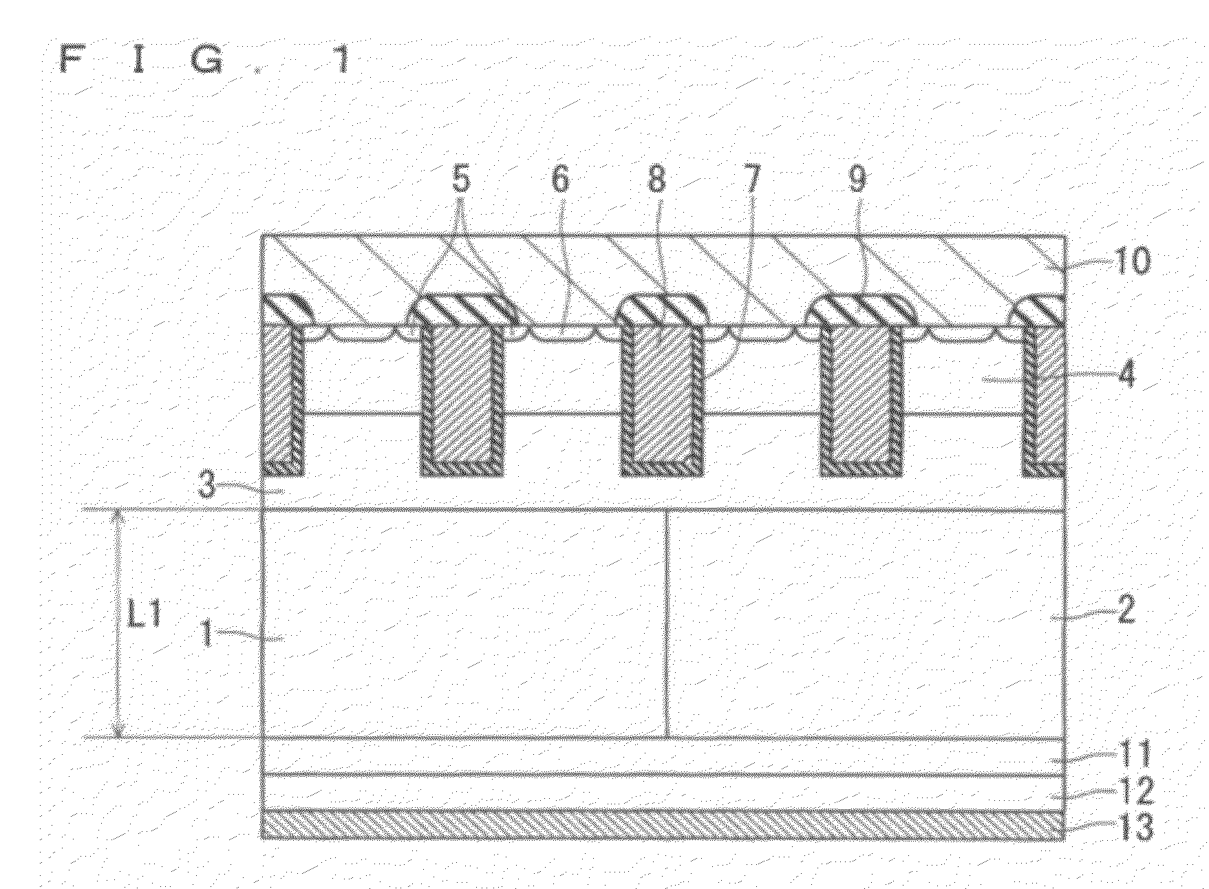
[0058]FIG. 4 is a cross-sectional view illustrating the structure of an IGBT according to a second preferred embodiment. It differs from the structure of the first preferred embodiment in that the first drift layer is formed of a super junction structure in which an N-drift layer 1, an insulating layer 14 such as SiO2, and a P-drift layer 2 are repeated in the horizontal direction in the drawing. The thicknesses of the N-drift layers 1, insulating layers 14, and P-drift layers 2 are all L2.
[0059]In the super junction structure, N-drift layers 1, insulating layers 14, and P-drift layers may be regularly repeated in this order in the horizontal direction, or insulating layers 14 may be inserted in arbitrary positions between the N-drift layers 1 and P-drift layers 2.
[0060]In the other respects, the structure is the same as that of the first preferred embodiment, and so the same description is not repeated.
Operation
[0061]Basic operation is the same as that of the first prefe...
third preferred embodiment
Preliminary Explanation
[0071]When an inverter circuit is switched with an inductive load such as an electric induction machine, as shown in FIG. 18, a free-wheel diode must be provided between the collector and emitter of IGBT in order to circulate the large current flowing in the inductive load between the load and the arm's closed circuit. Accordingly, RC-IGBT in which IGBTs and free-wheel diodes are provided in one chip is proposed.
[0072]FIG. 19 shows a cross-sectional view of an RC-IGBT according to a precondition of this preferred embodiment. In the trench gate RC-IGBT shown in FIG. 19, an N-drift layer 1 is formed on a P collector layer 12, and a P base layer 4 is formed on the N-drift layer 1. N emitter layers 5 and P-contact layers 6 are formed in the surface of the P base layer 4.
[0073]Also, trenches are formed from the surface of the P base layer 4 to a certain depth in the N-drift layer 1, and a gate electrode 8 is formed in each trench with an insulating gate film 7 the...
PUM
 Abstract
Description
Claims
Application Information