ESD protection structure for 3D IC

a protection structure and three-dimensional technology, applied in the direction of semiconductor devices, electrical equipment, semiconductor/solid-state device details, etc., can solve the problems of increased production cost, damage to the 3d ic or the tsv device, and complicated fabrication of the 3d ic, so as to reduce the fabrication cost of the ic

Inactive Publication Date: 2012-06-21
NAT CHIAO TUNG UNIV
View PDF6 Cites 36 Cited by
  • Summary
  • Abstract
  • Description
  • Claims
  • Application Information

AI Technical Summary

Benefits of technology

[0009]The invention is directed to an electrostatic discharge (ESD) protection structure for a three-dimensional (3D) integrated circuit (IC), which can effectively achieve ESD protection, and meanwhile reduce fabrication cost of the IC.

Problems solved by technology

(FIM) can be transmitted to the stacked chips through the TSV, which may cause a damage of the 3D IC or the TSV device.
Although such method may protect the 3D IC, fabrication steps of the 3D IC are increased, so that fabrication of the 3D IC is more complicated, and a production cost thereof is increased.

Method used


Image

  • ESD protection structure for 3D IC
  • ESD protection structure for 3D IC
  • ESD protection structure for 3D IC

Examples


Embodiment Construction

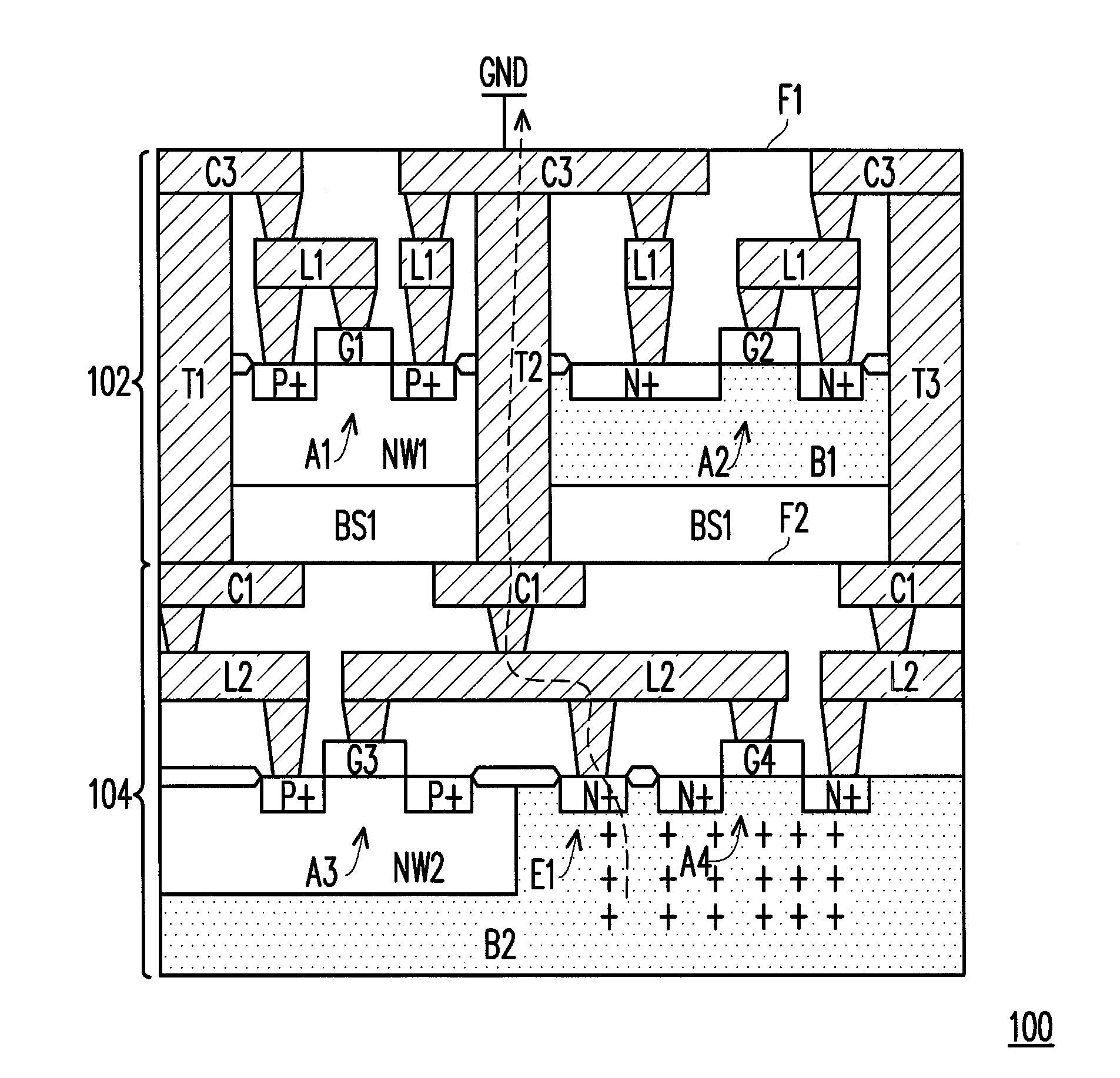
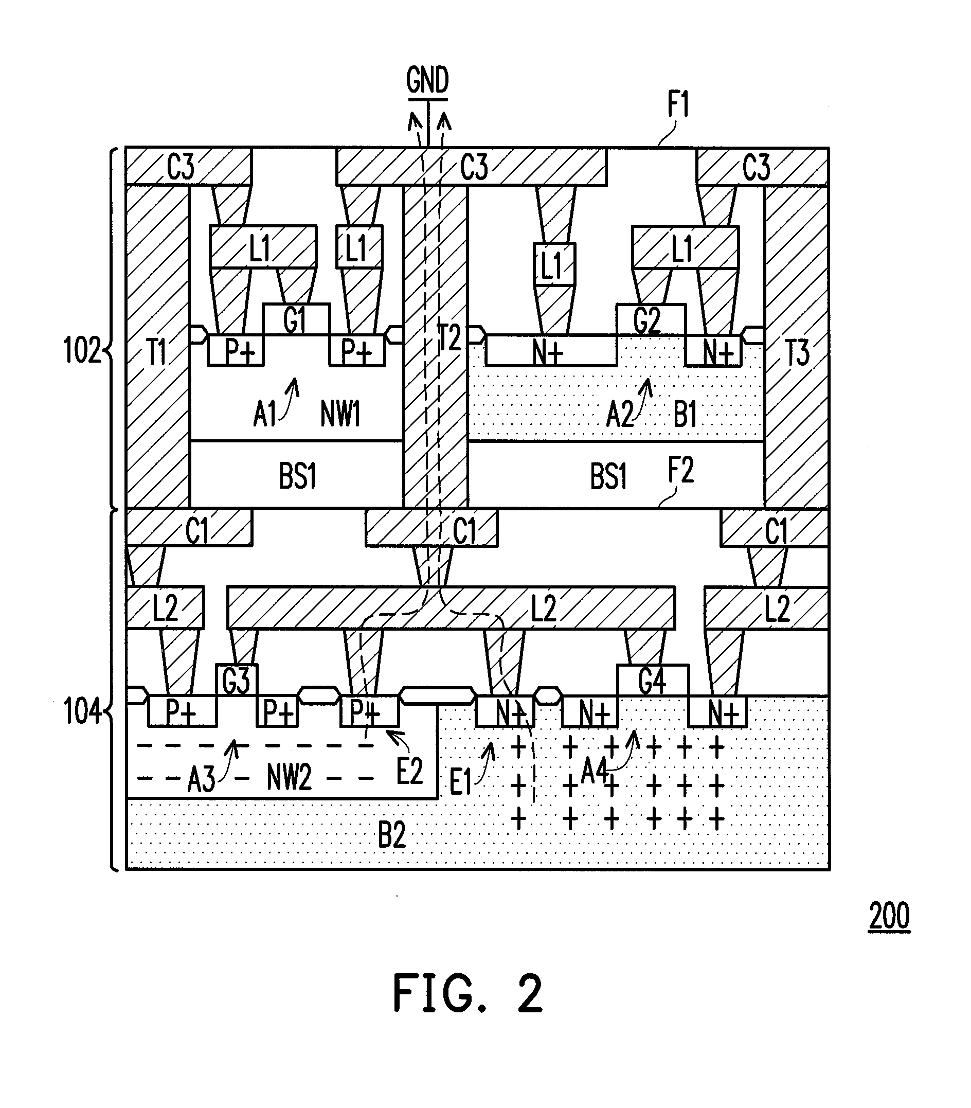
[0027]A concept of the invention is to combine a through-silicon via (TSV) device and an electrostatic discharge (ESD) protection device of a three-dimensional (3D) integrated circuit (IC) to protect the 3D IC and the TSV device from being damaged by the electrostatic discharge.

[0028]A plurality of embodiments is provided below to describe applications of the invention, though the invention may, however, be embodied in many different forms and should not be construed as being limited to the embodiments set forth herein; rather, these embodiments are provided so that this disclosure will be thorough and complete, and will fully convey the concept of the invention to those skilled in the art. In the accompanying drawings, sizes of different layers and regions and relative sizes are probably exaggerated for clarity. For simplicity's sake, only a structure of the invention is illustrated in each of the drawings, and other circuit components on the substrate are not illustrated, though t...


PUM


Abstract

An electrostatic discharge (ESD) protection structure for a 3D IC is provided. The ESD protection structure includes a first active layer, a through-silicon via (TSV) device and a second active layer. The TSV is disposed in the first active layer, and the second active layer is stacked with the first active layer. The second active layer includes a substrate and an ESD protection device, wherein the ESD protection device having a doping area embedded in the substrate, and the ESD protection device electrically connects the TSV device.

Description

CROSS-REFERENCE TO RELATED APPLICATION[0001]This application claims the priority benefit of Taiwan application serial no. 99144817, filed on Dec. 20, 2010. The entirety of the above-mentioned patent application is hereby incorporated by reference herein and made a part of this specification.BACKGROUND[0002]1. Field of the Invention[0003]The invention relates to an electrostatic discharge (ESD) protection structure. Particularly, the invention relates to an ESD protection structure for a three-dimensional (3D) integrated circuit (IC).[0004]2. Description of Related Art[0005]Along with complexity improvement of circuit designs and rapid development of semiconductor fabrication processes, and demand for circuit performance, integrated circuits (ICs) are developed to have a three-dimensional (3D) structure, so as to increase the circuit performance. Moreover, since different process techniques can be used in different layers of the 3D circuit, different processes can be used according t...

Claims


Application Information

Patent Timeline
Patent Type & Authority Applications(United States)
IPC IPC(8): H01L29/06
CPCH01L27/0296H01L23/481H01L2924/0002H01L2924/00H01L27/04H01L23/60
Inventor CHEN, KUAN-NENGLAI, MING-FANGCHEN, HUNG-MING
Owner NAT CHIAO TUNG UNIV
Why Eureka
Try Eureka