Large area light emitting electrical package with current spreading bus

a technology of light-emitting electrical packages and current-spreading buses, which is applied in the direction of discharge tubes/lamp details, discharge tubes luminescnet screens, organic semiconductor devices, etc., and can solve problems such as moisture and/or oxygen over tim

Active Publication Date: 2012-06-21
BOE TECH GRP CO LTD
View PDF0 Cites 10 Cited by
  • Summary
  • Abstract
  • Description
  • Claims
  • Application Information

AI Technical Summary

Problems solved by technology

Such panels should be hermetically sealed since moisture and oxygen have an adverse impact on the

Method used


Image

  • Large area light emitting electrical package with current spreading bus
  • Large area light emitting electrical package with current spreading bus
  • Large area light emitting electrical package with current spreading bus

Examples


Embodiment Construction

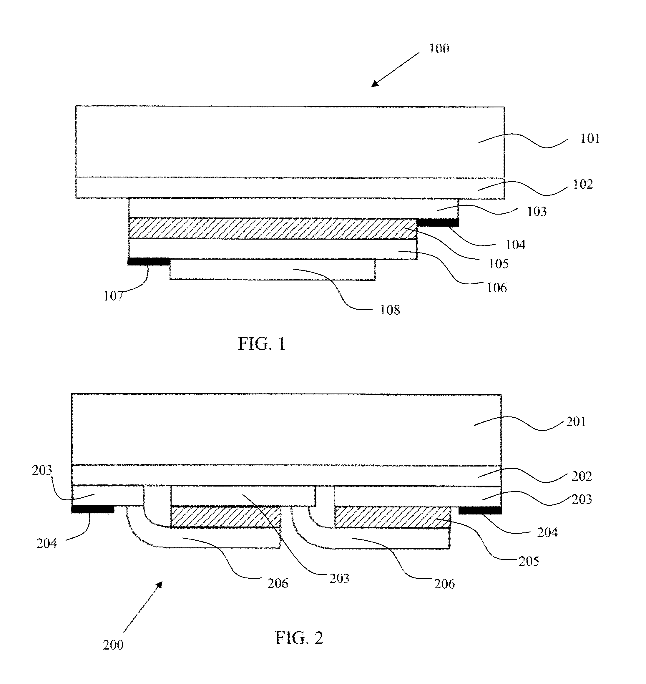
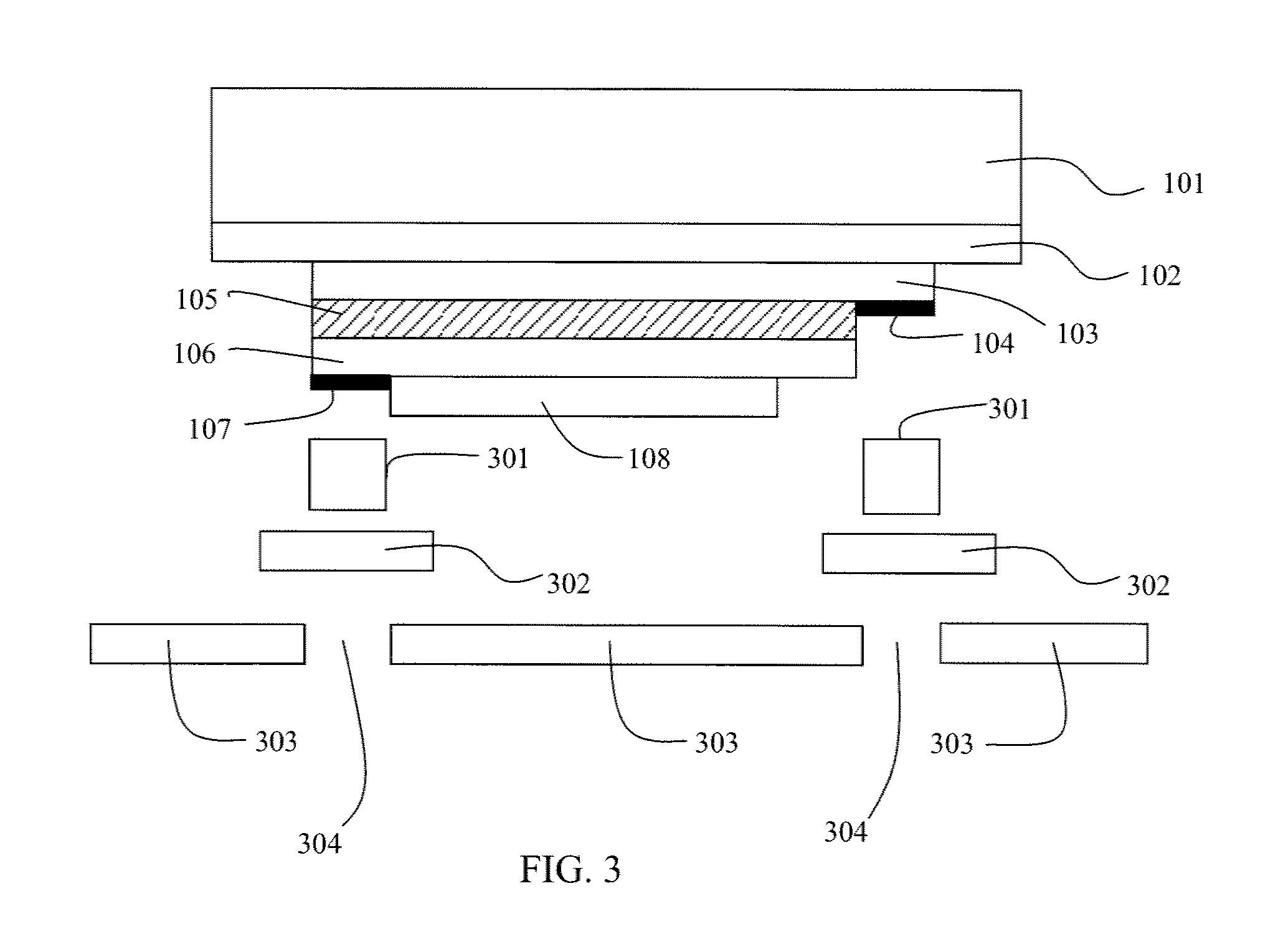
[0019]Applicants of the present invention have found that there may sometimes be a problem with large area, planar flexible OLED devices that employ transparent anodes. As such devices become large, current may not always be effectively spread from the point of current injection into the transparent anode layer, due to the relatively high sheet resistance for most transparent nonmetallic conductive materials, such as indium tin oxide (ITO). The current level may be high at the point of current injection, but is lowered elsewhere due to this sheet resistance. This sheet resistance can be as high as 50 ohm / sq or higher.

[0020]Current spreading along the transparent anode layer in the OLED presents a brightness uniformity issue for large-area devices. This creates areas of localized high current where a contact pad is connected to the external circuit, which results in those areas having an increase in luminance compared to the rest of the device. The relatively high sheet resistance of...


PUM


Abstract

Disclosed herein is a light emitting electrical package having a first electrode layer comprising a substantially transparent nonmetallic conductive material, and a plurality of light emitting elements disposed on said first electrode layer. The first electrode layer comprises a peripheral region, and an elongated bus is disposed on at least a portion of the peripheral region and adjacent the first electrode layer. The elongated bus is configured to spread current across a length dimension of said first electrode layer. Also disclosed are elongated bus structure designed intended to reduce the resistive losses along a transparent nonmetallic conductive contact at its edge or periphery. One design for an elongated bus comprises: (1) a conductive adhesive/metal foil/conductive adhesive sandwich structure; (2) another design comprises a vapor deposited bus of one or more materials; and a further design employs (1) and (2) in tandem.

Description

FIELD OF THE INVENTION[0001]The present disclosure relates to light emitting electrical packages, and particularly the present disclosure relates organic light emitting electrical packages with enhanced current spreading along a transparent conductive electrode.BACKGROUND[0002]Organic light emitting diode devices, or OLED devices, are generally known in the art. An OLED device typically includes one or more organic light emitting layer(s) disposed between electrodes. For example, first and second electrodes, such as a cathode and a light transmissive anode are formed on a substrate. Light is emitted when current is applied across the cathode and anode. As a result of the electric current, electrons are injected into the organic layer from the cathode and holes may be injected into the organic layer from the anode. Electrons and holes generally travel through the organic layer until they recombine at a luminescent center, typically an organic molecule or polymer. The recombination pr...

Claims


Application Information

Patent Timeline
IPC IPC(8): H01J1/62H05B44/00
CPCH01L27/3204H01L27/3237H01L2251/5361H01L51/5212H01L27/3288H10K59/86H10K59/10H10K59/179H10K50/814H10K2102/351
Inventor AURONGZEB, DEEDERKOSTKA, JAMES MICHAEL
Owner BOE TECH GRP CO LTD
Why Eureka
Try Eureka