

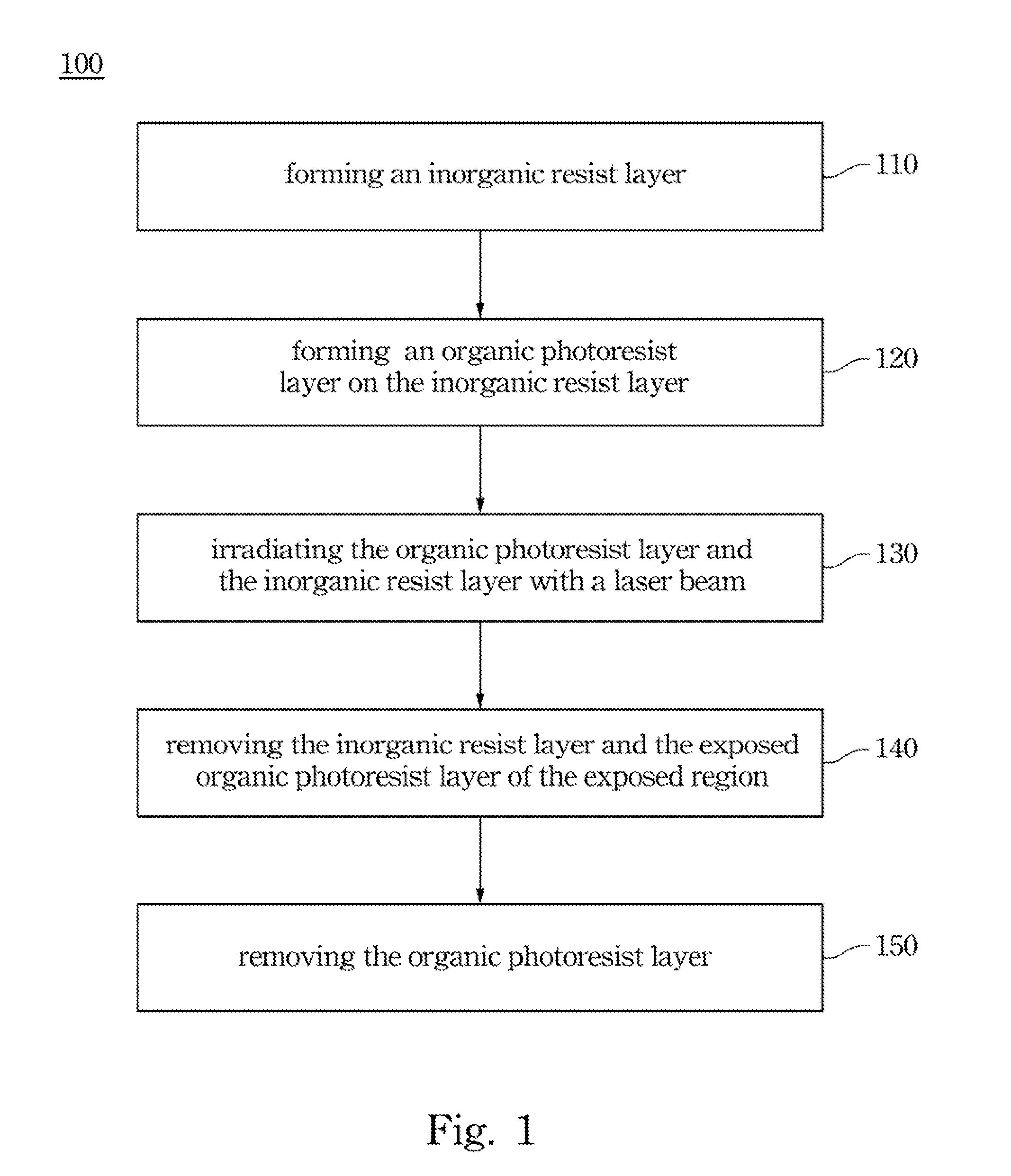
Nano-fabrication method
a technology of nanofabrication and nano-fabrication, applied in the field of nano-fabrication, can solve the problems of ineffective approach cost, inorganic resist, and high cost of the short-wavelength laser exposure system
- Summary
- Abstract
- Description
- Claims
- Application Information
AI Technical Summary
Benefits of technology
Problems solved by technology
Method used
Image

Examples
example
Patterning an Inorganic Resist Layer by Combining an Organic Photoresist
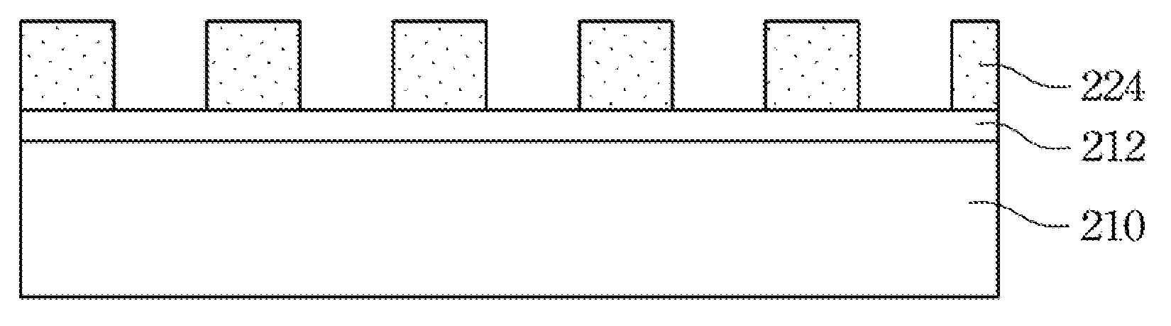
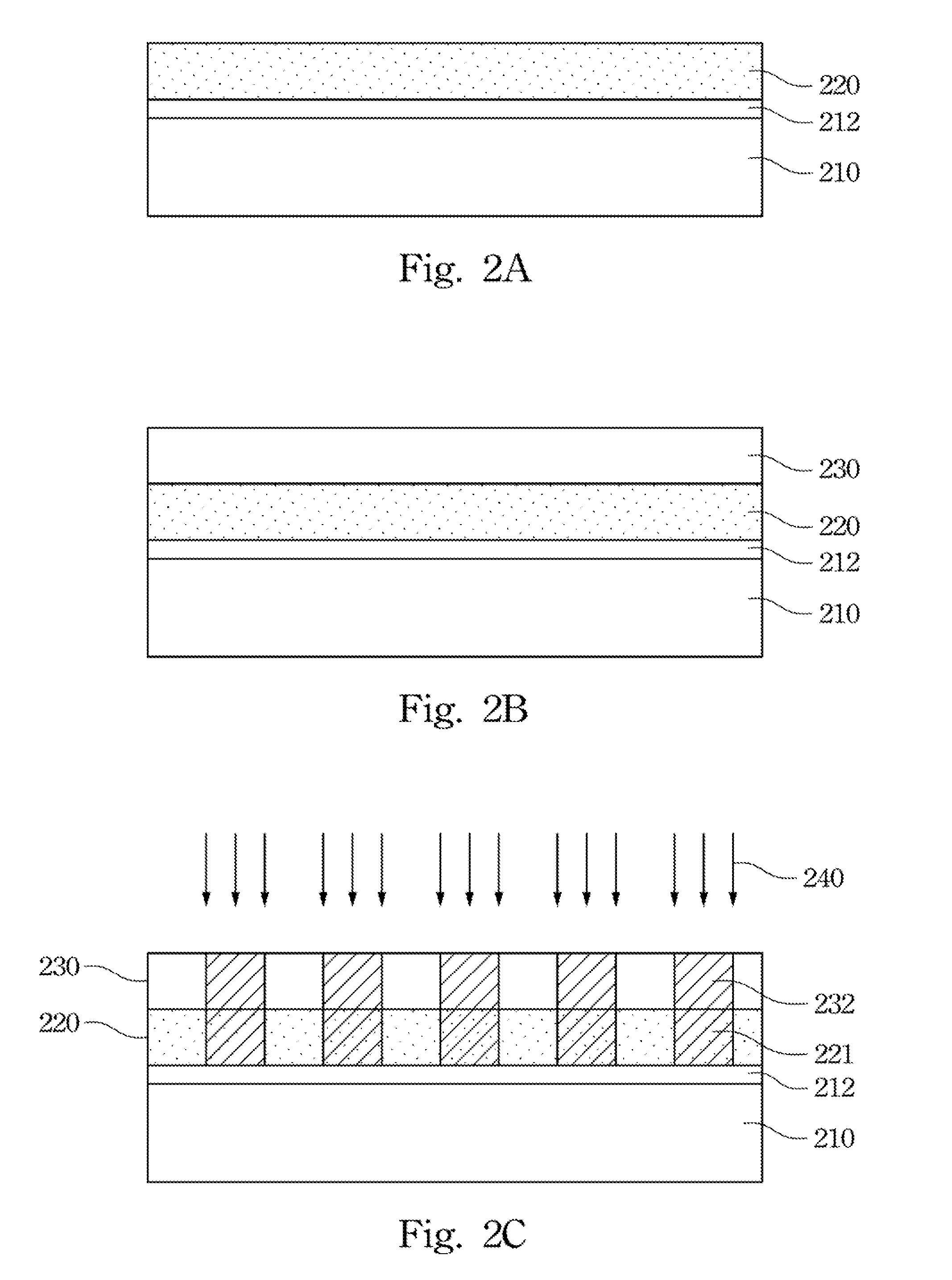
[0053]A 20 nm silicon layer, as a light absorption layer, was deposited on a glass substrate by sputtering in an argon (Ar) atmosphere at a pressure of 0.5 Pa. During the silicon sputtering, a DC source of 350 W was used and the Ar flow rate was 30 sccm. Next, an inorganic resist layer about 20 nm in thickness was deposited on the silicon layer, by sputtering, using a Ge13.5Sb40Sb46.5 target in an argon-oxygen mixed atmosphere (Ar / O2=5 / 1) at a pressure of 0.8 Pa. Subsequently, a novolac-type photoresist was coated on the inorganic resist layer by spin costing, and followed by a baking process at a temperature of 130° C. for 900 seconds. An organic photoresist layer about 25 nm in thickness was formed on the inorganic resist layer.
[0054]The substrate coated with the organic photoresist layer was exposed to a laser beam with a wavelength of 405 nm. The exposure was carried out with an irradiation power of 3.2 mW a...
PUM
| Property | Measurement | Unit |
|---|---|---|
| thickness | aaaaa | aaaaa |
| thickness | aaaaa | aaaaa |
| thickness | aaaaa | aaaaa |
Abstract
Description
Claims
Application Information