Image sensor IC

a technology of image sensor and pixel, applied in the field of image sensor, can solve the problems of increasing manufacturing costs, inability to achieve sufficient uniformity, and inability to achieve photoelectric conversion characteristics, etc., to suppress the variation in the photoelectric conversion characteristic of pixels, uniform film thickness, and the effect of constant formation speed and film quality of protective film formed on each of the pixels

Active Publication Date: 2012-06-28
ABLIC INC
View PDF0 Cites 0 Cited by
  • Summary
  • Abstract
  • Description
  • Claims
  • Application Information

AI Technical Summary

Benefits of technology

[0015]With those measures, each potential of regions which become a base at the time of forming the protective film can be set to be substantially constant over the entire pixel regions. Accordingly, a formation speed and film quality of the protective film formed on each of the pixels can be kept constant, whereby the protective film formed on each of the pixels has a substantially uniform film thickness and film quality. Consequently, the intensity of light incident on the photodiode of each of the pixels can be kept constant, thereby suppressing the variation in photoelectric conversion characteristic of the pixels, and obtaining an image sensor IC having the uniform photoelectric conversion characteristic over the entire IC.

Problems solved by technology

In the image sensor IC having a plurality of pixels arranged in one IC chip, however, a problem arises in variation of the photoelectric conversion characteristic due to change in intensity of incident light caused by a variation in thickness of a protective film formed on top of each of the plurality of photodiodes 12 which forms the pixels.
Though countermeasure for the problem is proposed in which planalization is performed after formation of the protective film, and in which a second protective film is formed to obtain further uniformity in the film thickness, problems still remain in that, for example, the number of process steps increases, which results in an increase in manufacturing costs, and sufficient uniformity cannot still be obtained.

Method used


Image

  • Image sensor IC
  • Image sensor IC
  • Image sensor IC

Examples


first embodiment

[0021]FIG. 1 is a schematic top view showing pixel regions of an image sensor according to the present invention.

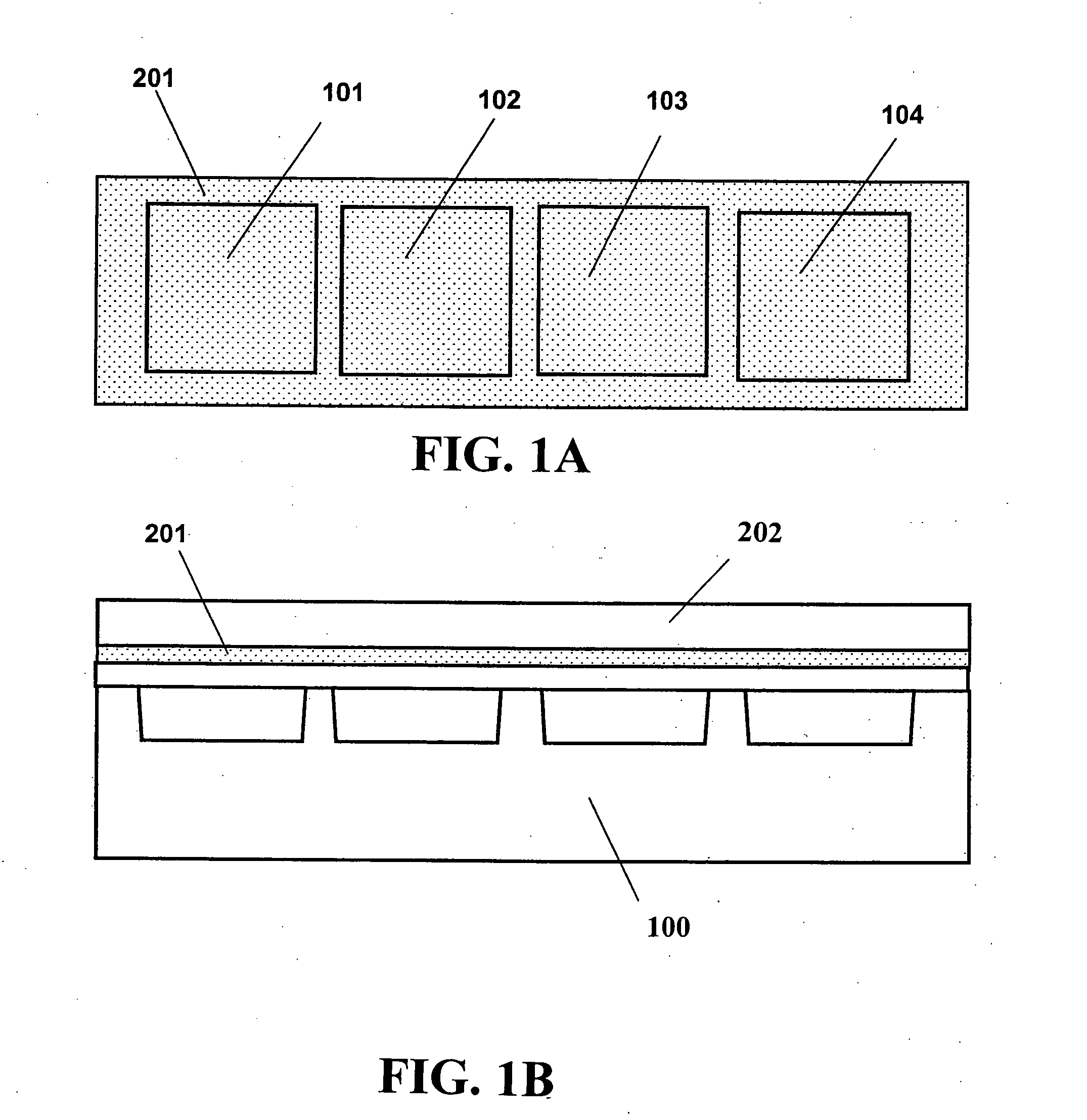
[0022]A plurality of pixel regions 101, 102, 103, and 104 are covered with a light-transmissive conducive material 201 for potential fixation, which is formed of a polycrystalline silicon thin film. The light-transmissive conductive material 201 covering the pixel regions 101, 102, 103, and 104 has the same potential as a whole. The light-transmissive conductive material 201 is electrically connected so as to hold the same potential as the substrate potential of the silicon substrate on which the image sensor is formed through the connection is not shown in FIG. 1. As a result, at the time of forming a protective film on the pixel regions thereafter, each potential of underlying pixel regions can be kept substantially constant over the entire pixel regions in the image sensor IC. Thus, a formation speed and film quality of the protective film formed on each pixel can also...

second embodiment

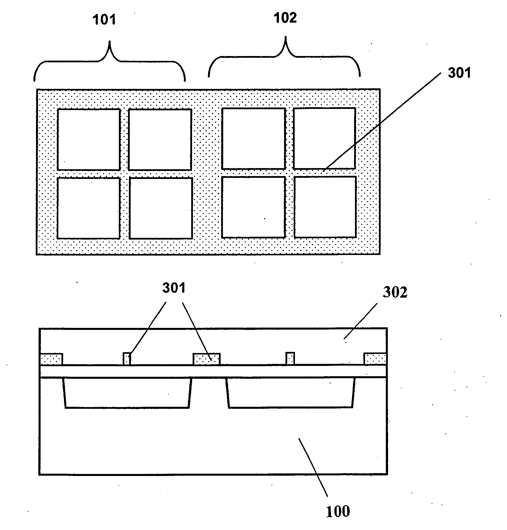
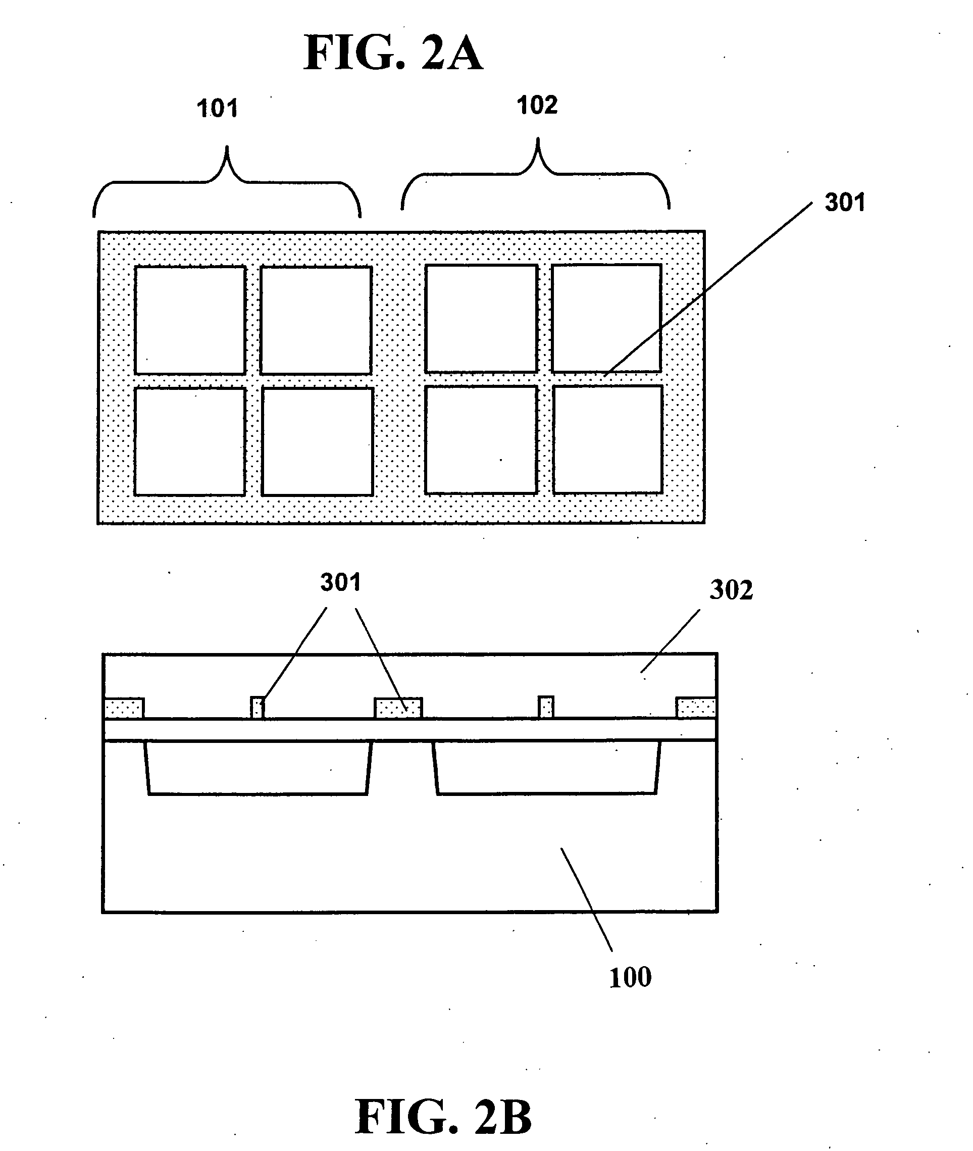
[0025]FIG. 2 is a schematic top view showing pixel regions of an image sensor according to the present invention.

[0026]The pixel region of the image sensor according to the first embodiment and that of the second embodiment are different from each other in the following point. In place of the shape of the light-transmissive conductive material 201 for potential fixation, which is formed of a polycrystalline silicon thin film or the like covering the pixel region 101, as shown in the example of FIG. 1, a light-transmissive conductive material 301 for potential fixation, which is formed of a polycrystalline silicon thin film or the like having a shape with an opening formed therein so as not to block the incident light into one pixel region 101, is formed in a cross shape in the second embodiment.

[0027]As described in the example of FIG. 1, the light-transmissive conductive material may be formed of a polycrystalline silicon thin film having a thickness of, for example, 2000 Å or smal...


PUM


Abstract

In a manufacturing method for an image sensor integrated circuit, a plurality of pixel regions each having a photodiode are arranged on a silicon substrate. A light-transmissive conductive film is formed over the silicon substrate. A protective film is formed on the light-transmissive conductive film while holding a potential of the light-transmissive conductive film at the same potential as that of the silicon substrate.

Description

BACKGROUND OF THE INVENTION[0001]1. Field of the Invention[0002]The present invention relates to an image sensor IC (integrated circuit) used in a device for capturing and transmitting image information, such as a facsimile, an image scanner, and an electronic camera.[0003]2. Description of the Related Art[0004]FIG. 3 is an exemplary circuit diagram for showing an image sensor of a related art. In a sensor circuit 10 of a MOS image sensor, a reset transistor 11 serving as a switching element for resetting a photodiode 12 to an appropriate voltage, and an amplifier circuit 13 for amplifying light induced charges accumulated in the photodiode 12 are connected to the photodiode 12 including a PN junction.[0005]Optical information can be obtained continuously through following three operations: a reset operation in which the reset transistor 11 is turned on so as to reset the photodiode 12 to a reset voltage to a satisfactory extent; an accumulation operation in which the reset transist...

Claims


Application Information

Patent Timeline
Patent Type & Authority Applications(United States)
IPC IPC(8): H01L27/146H01L31/10H04N1/028H04N5/335H04N5/369H04N5/374H04N5/3745
CPCH01L27/14692H01L27/14601H01L27/14H01L27/146
Inventor TAKASU, HIROAKI
Owner ABLIC INC
Why Eureka
Try Eureka