Emissive device and electronic apparatus having light transmitting portions of light shielding layer being smaller than partition opening

a technology of light shielding layer and emissive device, which is applied in the direction of discharge tube/lamp details, organic semiconductor devices, discharge tubes luminescnet screens, etc., can solve the problems of affecting accuracy, divergence of pencils of light, and disadvantageous variation of luminance and chromaticity in a single pixel, so as to achieve uniform quality in each pixel and enhance the directivity of pencils

Active Publication Date: 2010-11-23
SEIKO EPSON CORP
View PDF25 Cites 35 Cited by
  • Summary
  • Abstract
  • Description
  • Claims
  • Application Information

AI Technical Summary

Benefits of technology

[0010]An advantage of some aspects of the invention is that an emissive device has uniform quality in each pixel and enhanced directivity of pencils of light radiating to the outside. Another advantage of some aspects of the invention is that an electronic apparatus includes the emissive device.
[0012]According to an aspect of the invention, the light-transmitting portions of the light-shielding layer overlap the respective openings in the partition partitioning the light-emitting elements and each are smaller than the corresponding opening. Thus, pencils of light viewable from the outside are regulated by the light-transmitting portions of the light-shielding layer. The light-shielding layer masks peripheries of pixels. Even when luminance and chromaticity at the peripheries of the pixels close to the partition differ from those at middle portions of the pixels remote from the partition, nonuniformity in luminance and chromaticity in a single pixel is not visually identified because the peripheries of the pixels are masked with the light-shielding layer. Furthermore, the light-transmitting portions of the light-shielding layer overlap the respective opening in the partition partitioning the light-emitting elements and are each smaller than the corresponding opening. Thus, it is possible to enhance the directivity of the pencils of light radiating to the outside.
[0014]Preferably, the above-described emissive device further includes first electrodes; a second electrode; and a light-emitting sublayer disposed between the second electrode and the individual first electrodes, wherein each of the first electrodes is closer to the corresponding reflective layer than the second electrode, is composed of indium tin oxide (ITO), indium zinc oxide (IZO), or ZnO2, overlaps the corresponding reflective layer, and is wider than the corresponding reflective layer. A conductive oxide material, such as ITO, IZO, or ZnO2, having light transparency and conductivity can be used as electrodes for the light-emitting elements. Thus, the conductive oxide material can transmit light from the light-emitting elements to the reflective layers and can transmit light reflected from the reflective layers in the opposite direction. The first electrodes each composed of the conductive oxide material are patterned by etching with a strong acid, such as hydrogen bromide or hydrogen iodide. The reflective layers are each composed of a metal, such as aluminum, or other material having high reflectivity. Since each of the first electrodes overlaps the corresponding reflective layer and is wider than the corresponding reflective layer, it is possible to prevent the failure of the reflective layers caused by the use of a strong acid.
[0015]Preferably, color conversion layers for converting the color of light emitted from the light-emitting elements into different target colors are disposed at the respective light-transmitting portions, wherein the color conversion layers providing different target colors have different areas. Each of the color conversion layers may be a color filter that transmits more light of a predetermined wavelength range than light of other wavelength ranges. Alternatively, each of the color conversion layers may be composed of a photoluminescent material that receives light to emit another color of light. Luminous energy of the light-emitting elements is not uniform with respect to wavelengths of all colors. Degrees of conversion efficiency of the color conversion layers are different in response to the target colors. The term “conversion efficiency” means the ratio of the luminance of light incident on the color conversion layer to the luminance of outgoing light from the color conversion layer. Thus, even when a constant driving current is applied to light-emitting elements which have the same size and the same structure, the degrees of luminance of light converted through the color conversion layers are different in response to the types of color conversion layers, i.e., target colors. In consideration of spectrum properties of light incident on the color conversion layers and the conversion efficiency of the color conversion layers, luminous intensity (unit: candela), which is the product of luminance and an area, of each light-emitting element can be suitably set by changing the area of the corresponding color conversion layer in response to the target colors. Thereby, it is possible to improve image quality by striking a balance among the target colors.

Problems solved by technology

In these cases, luminance and chromaticity disadvantageously vary in a single pixel.
When the emissive device is used as an image display, the divergence of the pencils of light may affect viewability.
When the emissive device is used as an exposure device that is required to have high accuracy, the excess divergence of the pencils of light adversely affects accuracy.
Luminous energy of the light-emitting elements is not uniform with respect to wavelengths of all colors.

Method used


Image

  • Emissive device and electronic apparatus having light transmitting portions of light shielding layer being smaller than partition opening
  • Emissive device and electronic apparatus having light transmitting portions of light shielding layer being smaller than partition opening
  • Emissive device and electronic apparatus having light transmitting portions of light shielding layer being smaller than partition opening

Examples


Embodiment Construction

[0027]Embodiments of the invention will be described below with reference to the accompanying drawings. The drawings are not to scale.

Emissive Device

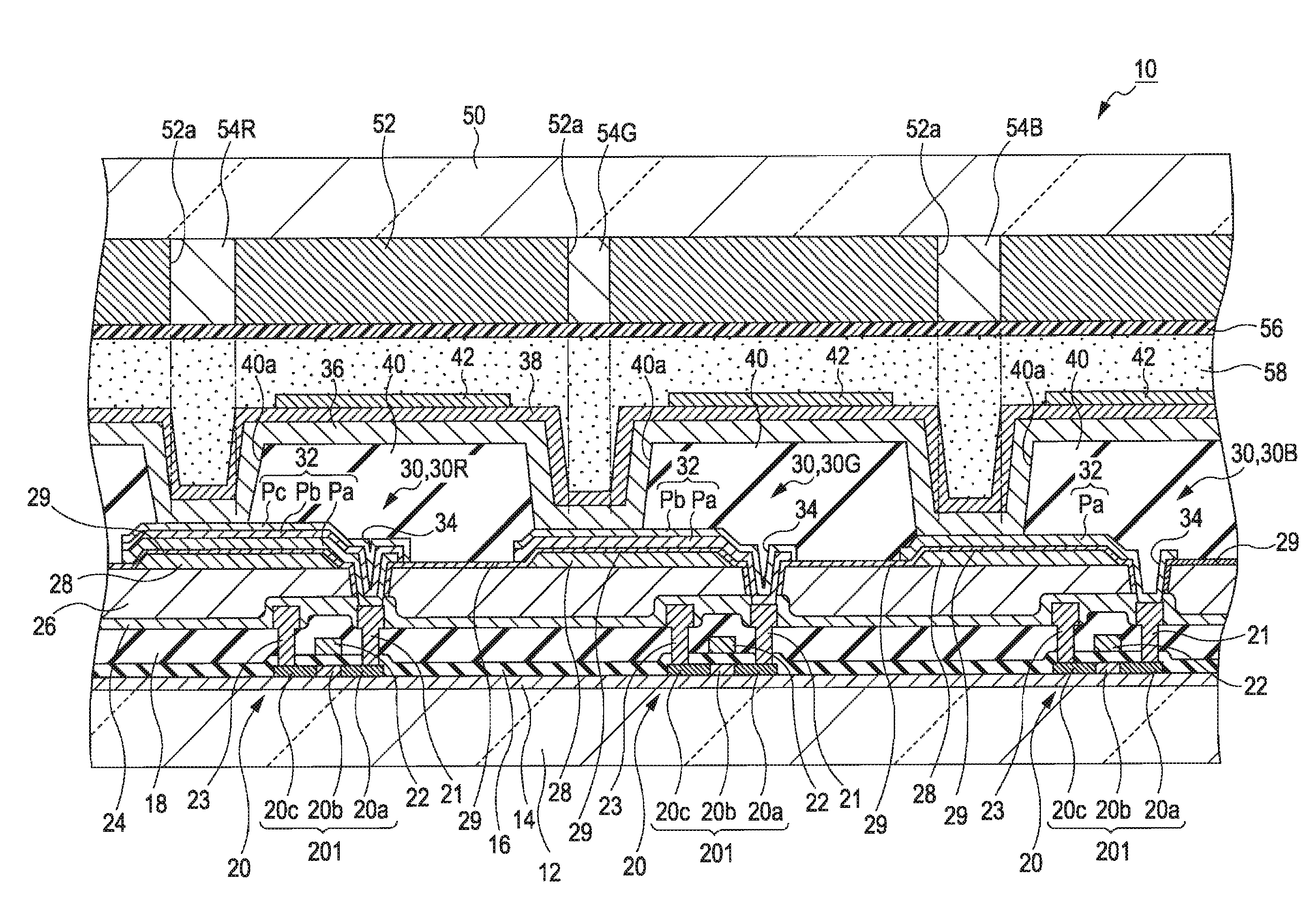
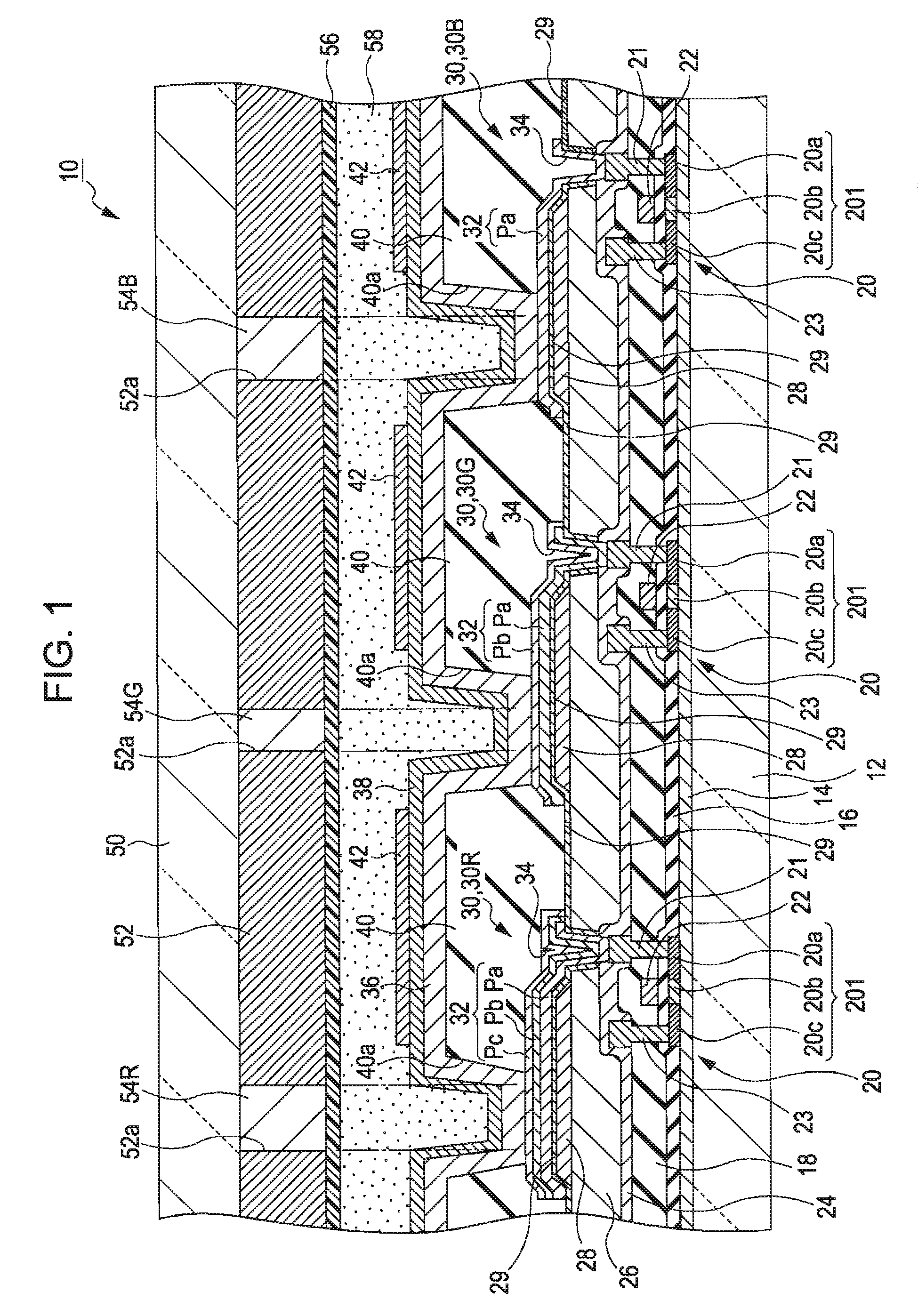
[0028]FIG. 1 is a fragmentary cross-sectional view of an emissive device 10 according to an embodiment of the invention. As shown in FIG. 1, the emissive device 10 includes a substrate 12 composed of, for example, glass or plastic. A substrate-protecting layer 14 mainly composed of silicon oxide is disposed on the substrate 12. A plurality of p-channel pixel transistors 20 are disposed on the substrate-protecting layer 14. The pixel transistors 20 are thin-film transistors (TFTs) and are arrayed in a matrix. The pixel transistors 20 are connected to respective light-emitting elements 30, which are described below, disposed on the substrate 12 to drive the light-emitting elements 30. That is, an active-matrix driving system is used in this emissive device 10. The emissive device 10 includes many light-emitting elements 30 and many pixel ...


PUM


Abstract

An emissive device includes a substrate; a plurality of light-emitting elements disposed on the substrate; a light-shielding layer opposite the substrate, the light-emitting elements being disposed between the substrate and the light-shielding layer, and the light-shielding layer having light-transmitting portions that transmit light emitted from the light-emitting elements; and a partition composed of an insulating material and disposed on the substrate, the partition partitioning the light-emitting elements and having openings each demarcating the light-emitting region of the corresponding light-emitting element, wherein each of the light-transmitting portions overlaps the corresponding opening and is smaller than the corresponding opening.

Description

[0001]The entire disclosure of Japanese Application No. 2006-003304, filed Jan. 11, 2006 is expressly incorporated by reference herein.BACKGROUND[0002]1. Technical Field[0003]The present invention relates to an emissive device including light-emitting elements, such as organic light-emitting diodes, which emit light having a luminance level corresponding to a current, and relates to an electronic apparatus including the emissive device.[0004]2. Related Art[0005]Electroluminescent (EL) elements that are excited by an electric field to emit light are one known example of light-emitting elements. In an emissive device including EL elements, many pixel circuits are arrayed in a matrix on a substrate, and one of the EL elements is disposed in each pixel circuit. Each EL element has a light-emitting layer disposed between an anode and a cathode. A hole injection layer or other layer is disposed between the anode and the cathode, in some cases.[0006]An example of such an emissive device is...

Claims


Application Information

Patent Timeline
Patent Type & Authority Patents(United States)
IPC IPC(8): H01J1/62
CPCH01L27/3244H01L51/5262H01L27/322H01L27/3246H01L2251/5315H10K59/38H10K59/12H10K59/122H10K50/85H10K2102/3026H05B33/22
Inventor KUBOTA, TAKEHIKOKANDA, EIJI
Owner SEIKO EPSON CORP
Why Eureka
Try Eureka