
Optical sensor and display device

Inactive Publication Date: 2012-07-05
SHARP KK
View PDF2 Cites 18 Cited by
  • Summary
  • Abstract
  • Description
  • Claims
  • Application Information

AI Technical Summary

Benefits of technology

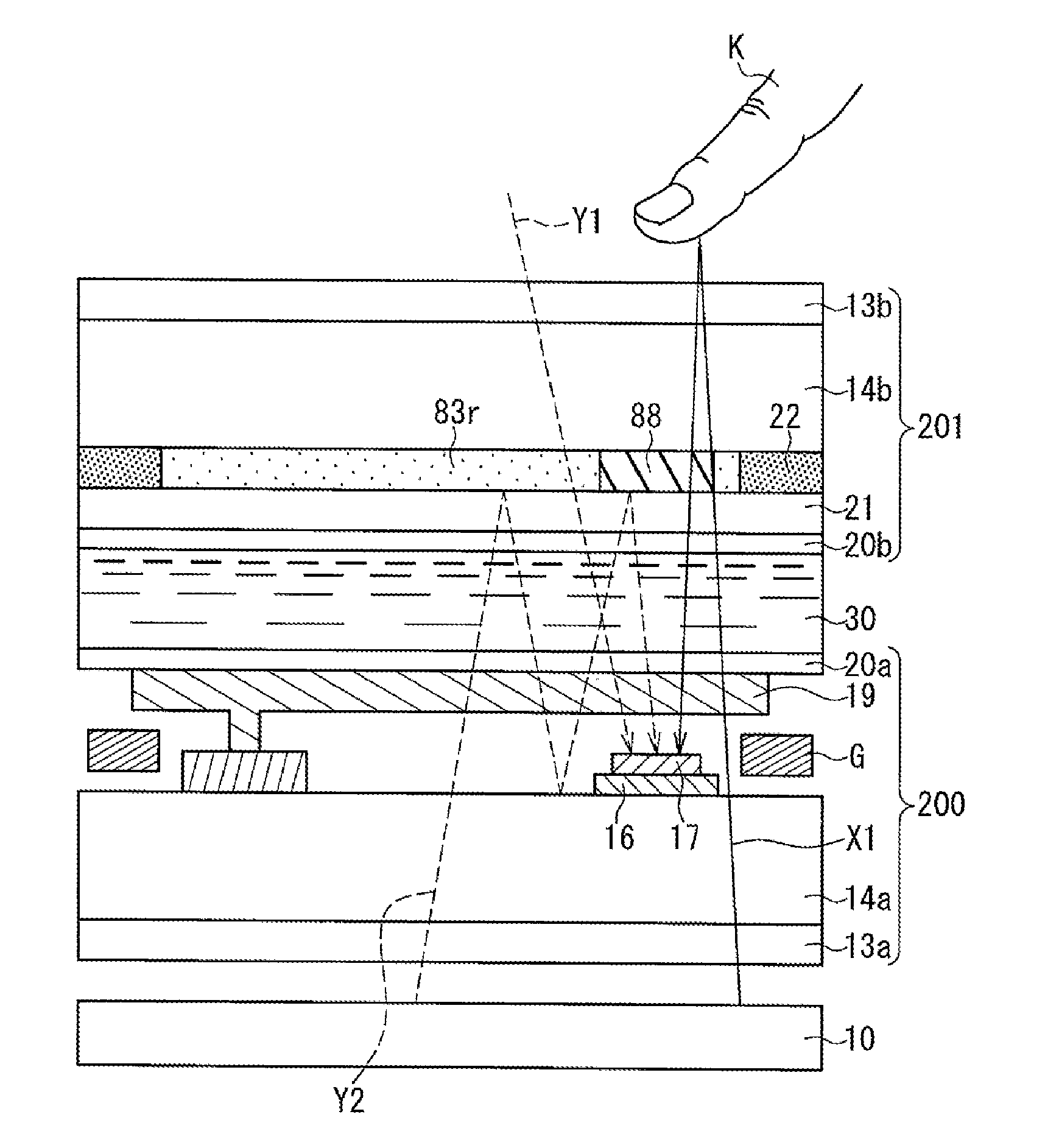
[0004]However, in the conventional sensor-equipped display device, a selective transmission filter that selectively transmits light in the non-visible light range is provided on a CF substrate, and a light receiving cell (sensor) is provided on a TFT substrate. Therefore, for example, in a step of laminating the CF substrate and the TFT substrate, the sensor and the selective transmission filter tend to be misaligned due to a positioning error. Through an interstice occurring due to this error, noise light such as external light is incident on the sensor. Besides, since a liquid crystal layer and the like are present between the sensor and the selective transmission filter, internal reflection light in the liquid crystal layer becomes light of a noise component, and is incident on the sensor. Such noise light causes an S / N ratio to decrease.
[0005]In light of this, it is an object of the present invention to provide an optical-sensor-equipped liquid crystal display device that is capable of reducing noise light incident on a photodetecting element and improving an S / N ratio.
[0007]The present invention makes it possible to reduce noise light incident on a photodetecting element and to improve the S / N ratio.

Problems solved by technology

Therefore, for example, in a step of laminating the CF substrate and the TFT substrate, the sensor and the selective transmission filter tend to be misaligned due to a positioning error.
Through an interstice occurring due to this error, noise light such as external light is incident on the sensor.
Besides, since a liquid crystal layer and the like are present between the sensor and the selective transmission filter, internal reflection light in the liquid crystal layer becomes light of a noise component, and is incident on the sensor.

Method used


Image

  • Optical sensor and display device
  • Optical sensor and display device
  • Optical sensor and display device

Examples


embodiment 1

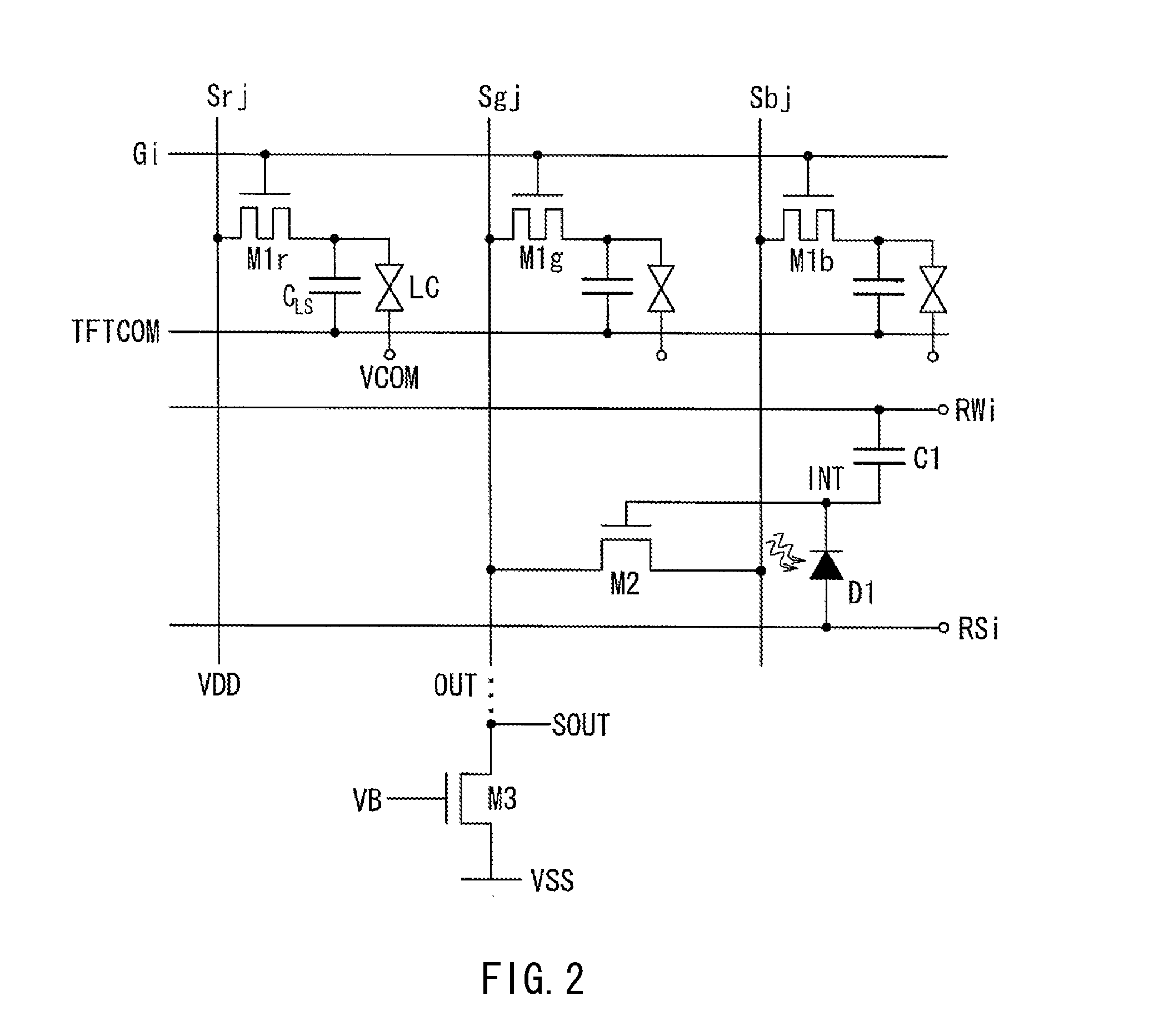
[0044]First, a configuration of a TFT substrate provided in a liquid crystal display device according to Embodiment 1 is explained, with reference to FIGS. 1 and 2.

Configuration of TFT Substrate

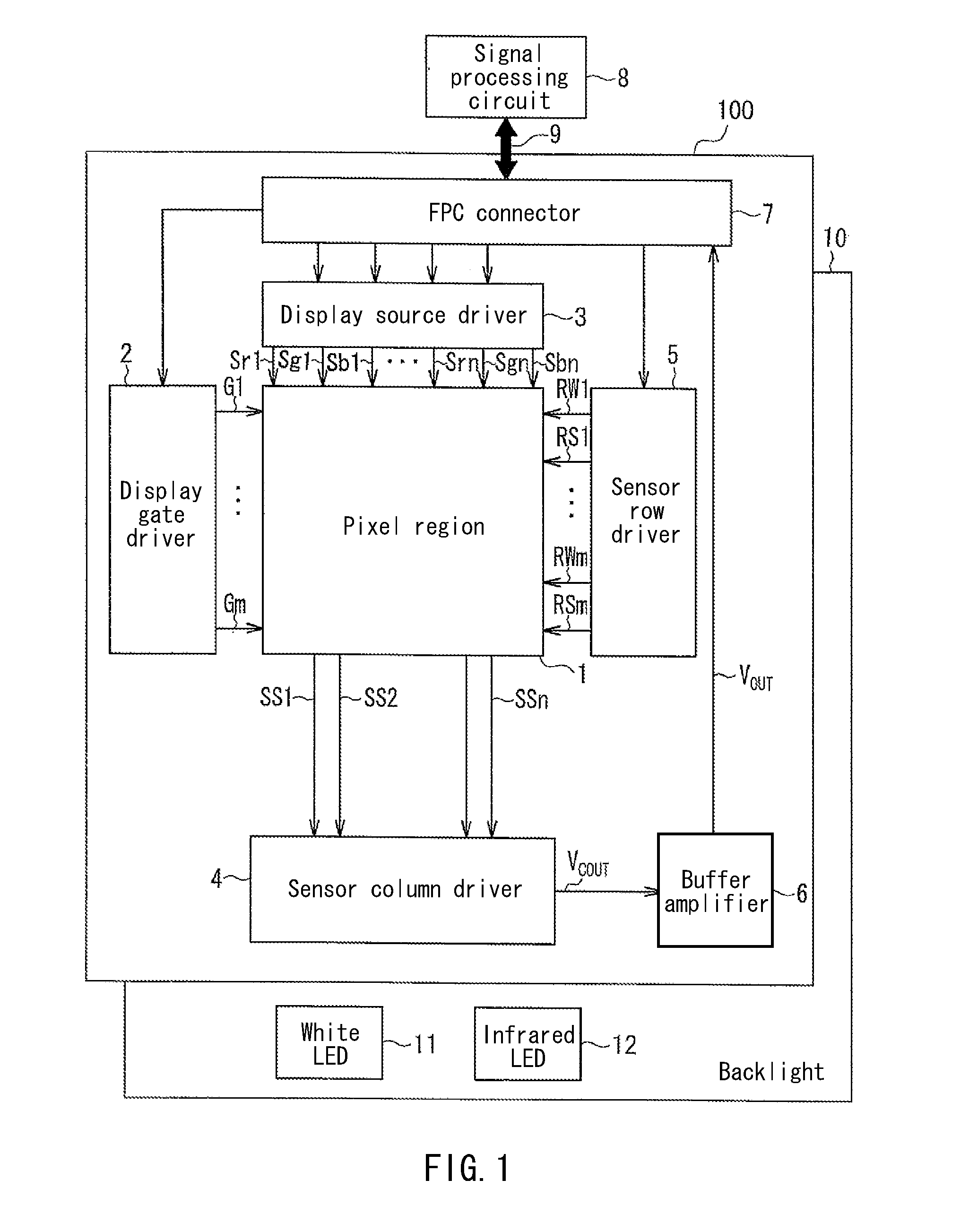
[0045]FIG. 1 is a block diagram showing a schematic configuration of a TFT substrate 100 provided in a liquid crystal display device according to Embodiment 1. As shown in FIG. 1, the TFT substrate 100 includes, on a glass substrate, at least a pixel region 1, a display gate driver 2, a display source driver 3, a sensor column driver 4, a sensor row driver 5, a buffer amplifier 6, and an FPC connector 7. Further, a signal processing circuit 8 for processing image signals captured by optical sensors (described later) in the pixel region 1 is connected to the TFT substrate 100 via the aforementioned FPC connector 7 and an FPC (flexible printed circuit) 9.

[0046]The pixel region 1 is a region where pixel circuits including a plurality of pixels for displaying images are formed. In the present em...

embodiment 2

[0095]FIG. 15 is a cross-sectional view of a liquid crystal display device according to Embodiment 2. The liquid crystal display device shown in FIG. 15 has a configuration obtained by adding an unwanted infrared light cut filter 18a to the configuration shown in FIG. 1, the cut filter 18a being provided so as to overlap the infrared light transmission filter 18. The unwanted infrared light cut filter 18a is a filter that cuts off light in a band that is unnecessary for the optical sensor, among light in the transmission band of the infrared light transmission filter 18. The unwanted infrared light cut filter 18a is formed with a filter in which a light absorbing material that absorbs infrared rays in a band unnecessary for the optical sensor is used. More specifically, the unwanted infrared light cut filter 18a contains, for example, an infrared light absorbing composition containing phosphoric acid ester. By laminating the unwanted infrared light cut filter 18a over the infrared l...

embodiment 3

[0099]FIG. 17A is a top view showing an area for one pixel in a pixel region 1 of a liquid crystal display device according to Embodiment 3. FIG. 17B is a cross-sectional view taken along a line x3-x′3 in FIG. 17A. FIG. 17C is a cross-sectional view taken along a line y3-y′3 in FIG. 17A. The color filter is provided in a TFT substrate 101a in the present embodiment, while, in Embodiment 1, the color filter is provided in the counter substrate 101. As shown in FIGS. 17A to 17C, in the TFT substrate 100a, an optical sensor is formed with a light shielding layer 16 provided on the glass substrate 14a, and a photodiode 17 provided on the light shielding layer 16. On the glass substrate 14a, TFTs, M1s, gate lines G, and source lines S that compose pixel circuits are formed also. In the TFT substrate 100a, further, an infrared light transmission filter 18 is provided so as to cover the photodiodes 17. On this infrared light transmission filter 18, green color filters 23g, blue color filte...


PUM


Abstract

In a liquid crystal display device, noise light to a photodetecting element is reduced, whereby an improved S / N ratio is achieved. The liquid crystal display device includes: a first substrate (100) on which a pixel circuit is provided; a second substrate (101) arranged so as to face the first substrate (100) with a liquid crystal layer (30) being interposed therebetween; a photodetecting element (17) provided on the first substrate (100); and a detection light filter (18) that is provided between the photodetecting element (17) and the liquid crystal layer (30) and that cuts off light in a band outside a signal light band that is a band of light to be detected by the photodetecting element (17).

Description

REFERENCE TO RELATED APPLICATIONS [0001]This application is the national stage under 35 USC 371 of International Application No. PCT / JP2010 / 064015, filed Aug. 19, 2010, which claims priority from Japanese Patent Application No. 2009-208476, filed Sep. 9, 2009, the entire contents of which are incorporated herein by reference.FIELD OF THE INVENTION [0002]The present invention relates to an optical sensor having a photodetecting element such as a photodiode or a phototransistor, and relates to a display device equipped with the optical sensor.BACKGROUND OF THE INVENTION[0003]Conventionally, an optical-sensor-equipped display device has been proposed that includes a photodetecting element, for example, a photodiode, in each pixel so as to be capable of detecting brightness of external light and capturing an image of an object that approaches a display thereof. Known as a configuration of such an optical-sensor-equipped display device is, for example, a configuration in which light is e...

Claims


Application Information

Patent Timeline
IPC IPC(8): G02F1/13357H01J9/26G02F1/1335
CPCG01J1/02G01J1/0204G01J1/0488G06F3/042G01J3/506G06F3/0412G01J1/46
Inventor YUKI, RYUZOUSUKURA, NARUKATOH, HIROMINEMOTO, TADASHISHIGETA, HIROAKIKANBAYASHI, YUICHI
Owner SHARP KK
Learn More