

Method of manufacturing a display substrate
- Summary
- Abstract
- Description
- Claims
- Application Information
AI Technical Summary
Benefits of technology
Problems solved by technology
Method used
Image

Examples
Embodiment Construction
[0037]Hereinafter, the claimed subject matter will be explained in detail with reference to the accompanying drawings.
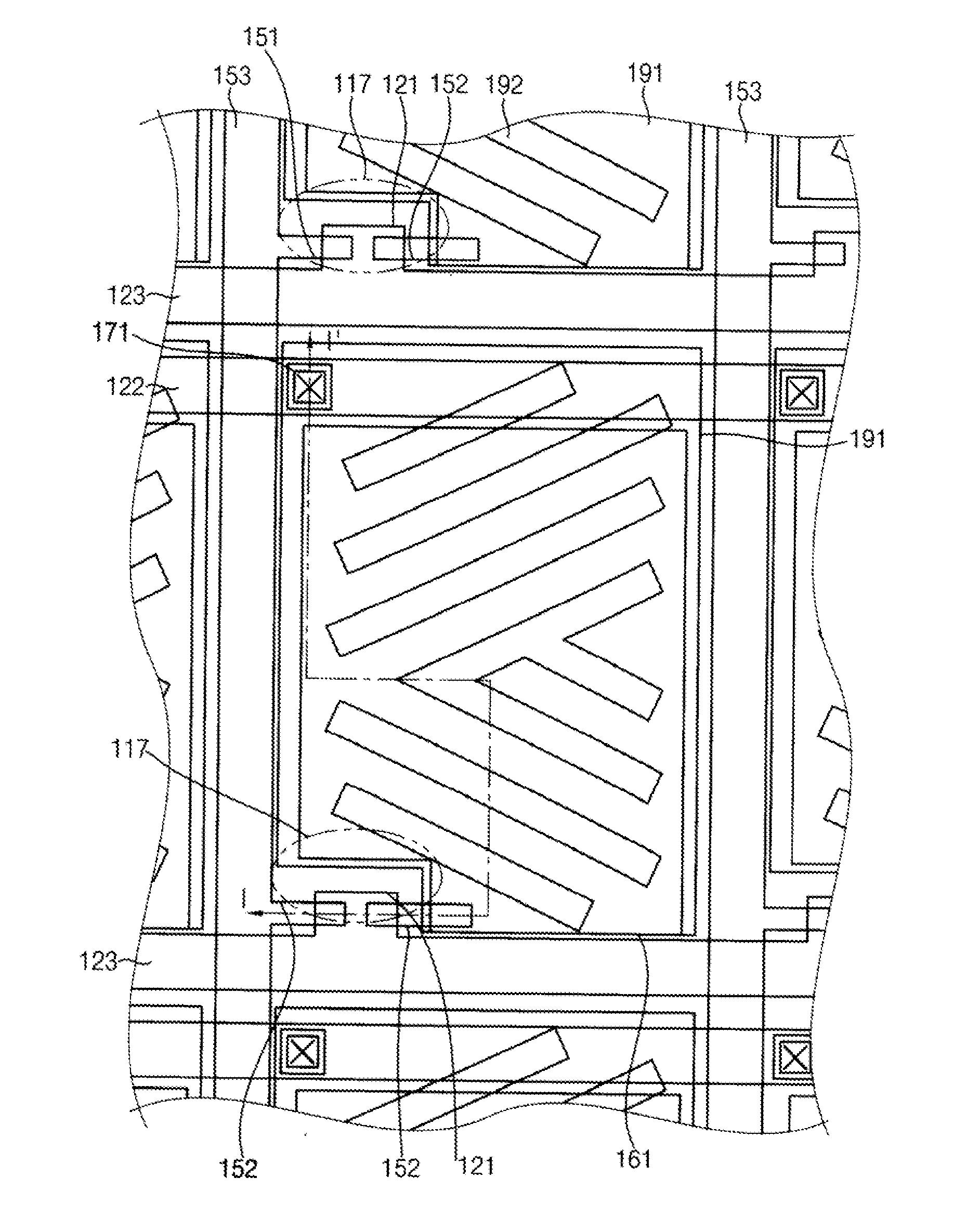
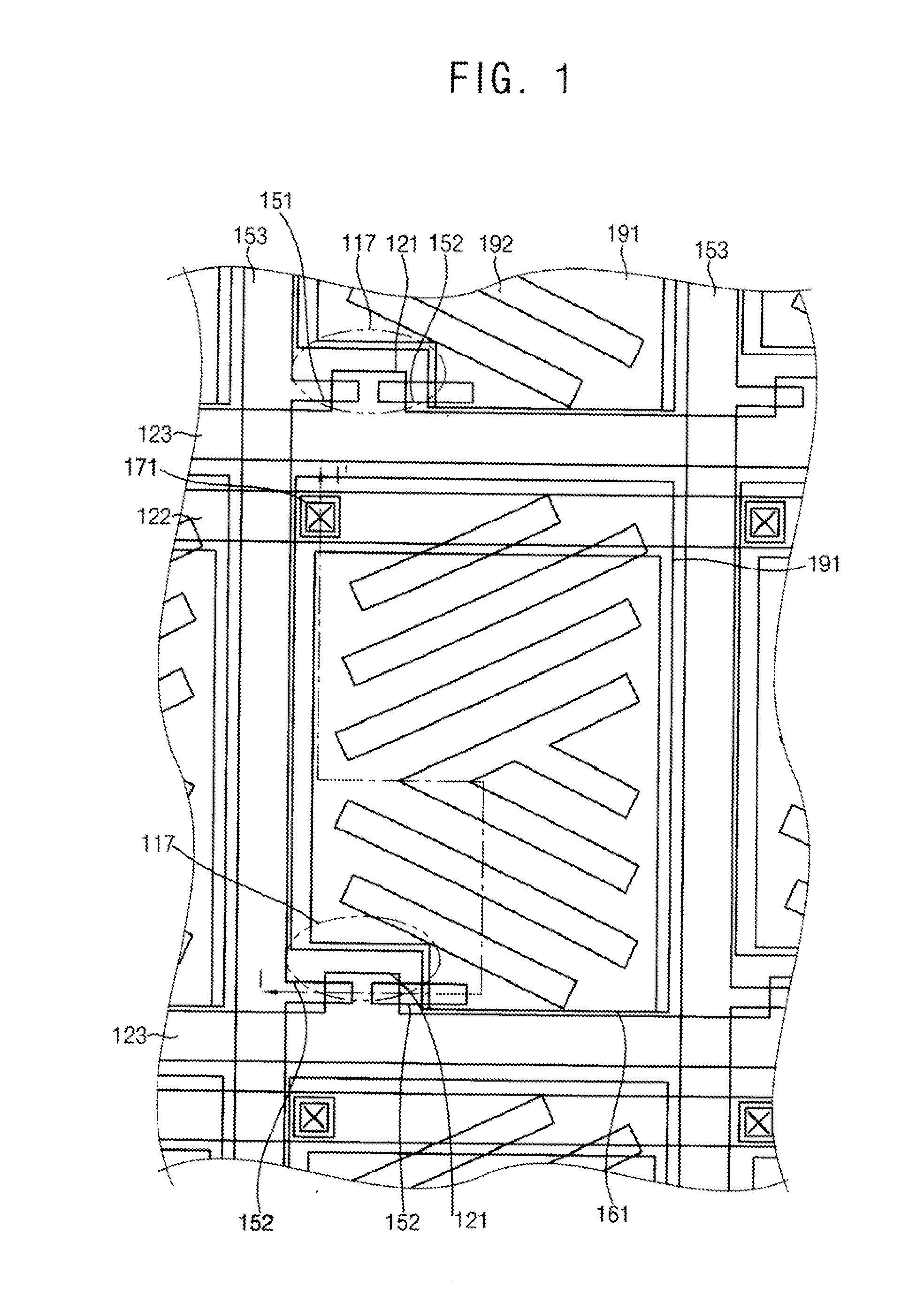
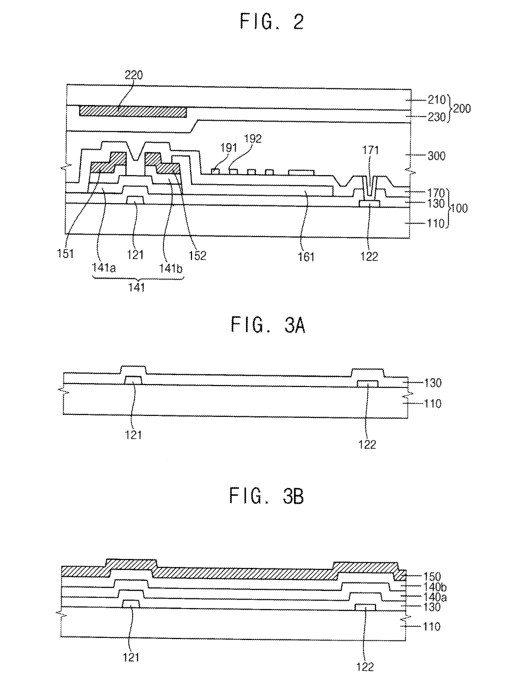
[0038]FIG. 1 is a plan view illustrating a display panel according to an example embodiment. FIG. 2 is a cross-sectional view illustrating the display panel taken along a line I-I′ of FIG. 1.
[0039]Referring to FIGS. 1 and 2, a display panel 100 includes a plurality of pixels. The pixels are defined by an area in which data and gate lines 153 and 123 cross each other and a pixel electrode is formed.
[0040]Each of the pixels includes a switching element 117 and first and second pixel electrodes 161 and 191. The switching element 117 includes a gate electrode 121, a semiconductor pattern 141, a source electrode 151, and a drain electrode 152.
[0041]The gate electrode 121, a common electrode line 122, and a gate line 123 are formed on a lower insulating substrate 110. The gate electrode 121 is extended from the gate line 123, and is formed in the pixel. The common electrod...
PUM
 Abstract
Description
Claims
Application Information