Noncontact determination of interface trap density for semiconductor-dielectric interface structures

a technology of interface trap density and semiconductordielectric interface, which is applied in the direction of individual semiconductor device testing, semiconductor/solid-state device testing/measurement, instruments, etc., can solve the problem of difficult and/or inviable determination of surface barrier potential as a function of surface charge applied to obtain the dependence of interface trap on surface charg

Active Publication Date: 2012-07-12
UNIV OF SOUTH FLORIDA
View PDF6 Cites 10 Cited by
  • Summary
  • Abstract
  • Description
  • Claims
  • Application Information

AI Technical Summary

Benefits of technology

[0007]Embodiments of the subject invention relate to a method and apparatus for determining the interface trap charge and / or interface trap density at a semiconductor-dielectric interface or a semiconductor-oxide interface. Specific embodiments can determine the interface trap density in a non-contact manner. A specific embodiment can determine the interface trap density of SiO2-4H—SiC structures. Specific embodiments of the subject method and apparatus can be used to characterize interfaces of any semiconductor-dielectric interfaces where rapid recovery to pre-illumination potential value after illumination with light, allowing quick modulation of the contact potential difference voltage of the structure, is not possible. For cases where rapid recovery after illumination of the structure is not possible, determination of the surface barrier potential as a function of charge applied to the surface needed to obtain the interface trap dependence on the surface charge is difficult and / or not viable. Semiconductor materials to which embodiments of the subject method and apparatus can be applied include, but are not limited to, SiC, GaN, GaAs, and wide bandgap semiconductors used in field effect structures. Embodiments of the invention can be utilized with semiconductors, for example n-type or p-type, having a range of doping densities, such as, but not limited to, 1011 / cm3 to 1018 / cm3. Specific embodiments can be utilized with n-type or p-type semiconductors having doping densities in the range 1014 / cm3 to 1018 / cm3.

Problems solved by technology

For cases where rapid recovery after illumination of the structure is not possible, determination of the surface barrier potential as a function of charge applied to the surface needed to obtain the interface trap dependence on the surface charge is difficult and / or not viable.

Method used


Image

  • Noncontact determination of interface trap density for semiconductor-dielectric interface structures
  • Noncontact determination of interface trap density for semiconductor-dielectric interface structures
  • Noncontact determination of interface trap density for semiconductor-dielectric interface structures

Examples


specific embodiments

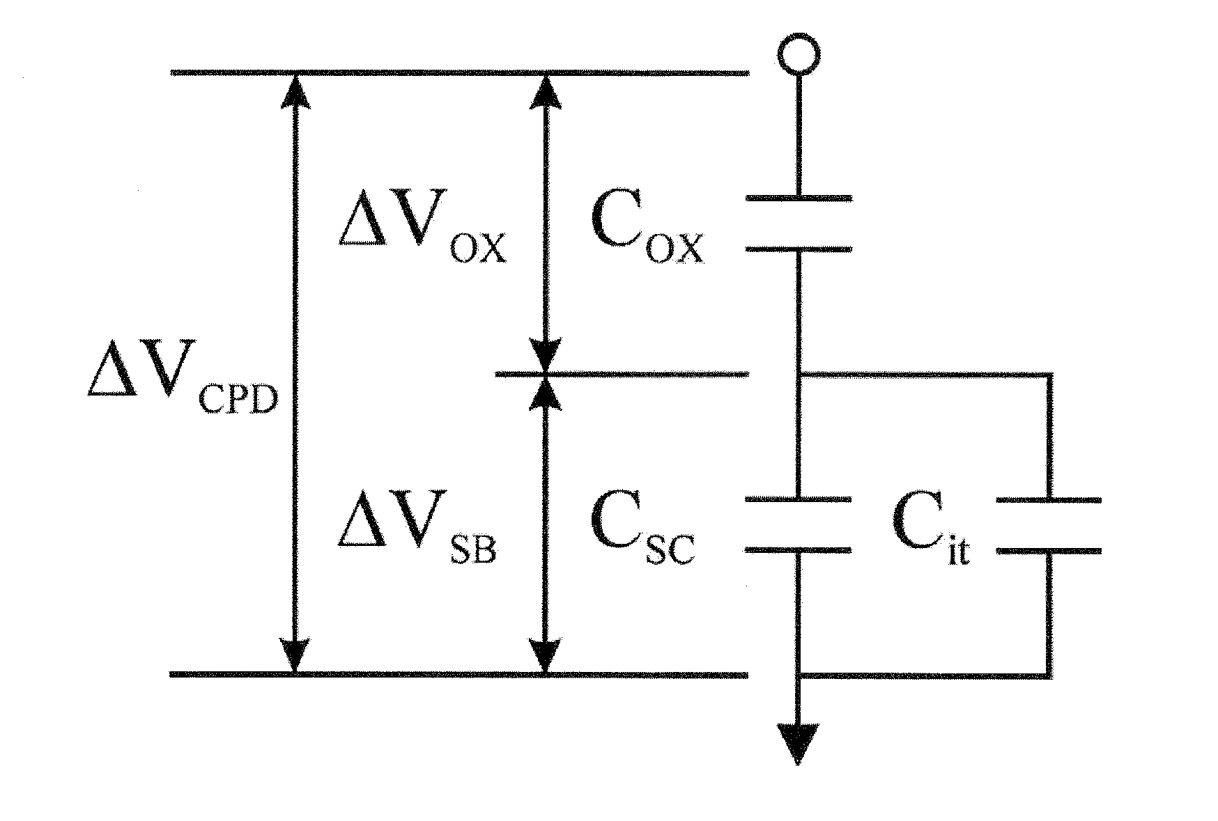
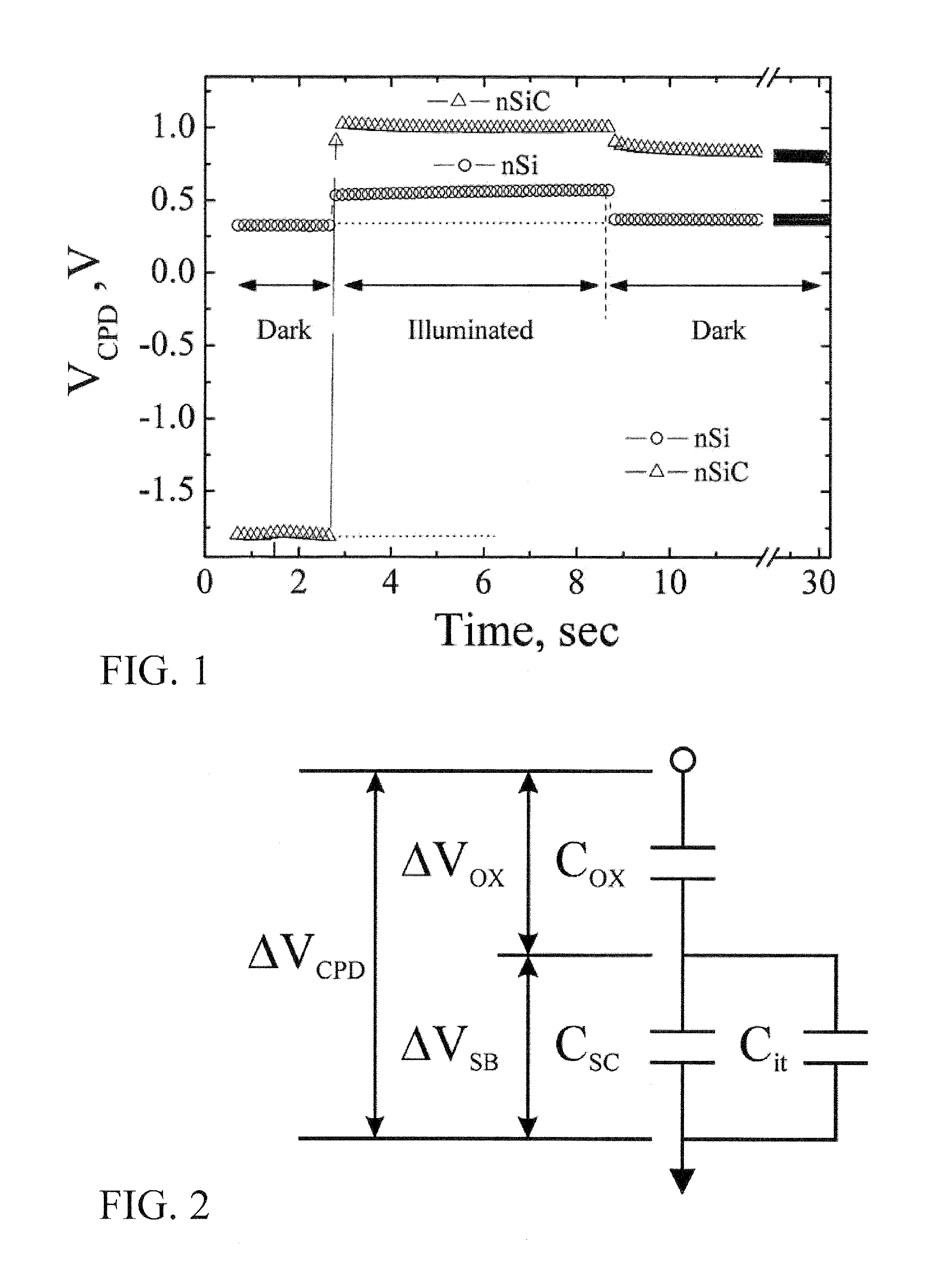
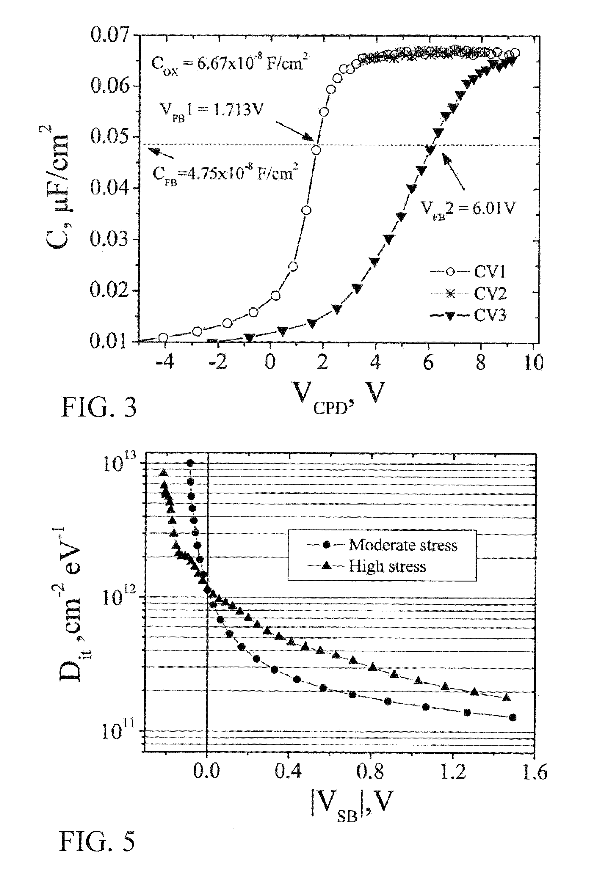
[0034]A specific embodiment 1 relates to a method of determining an interface trap density at an interface between a semiconductor and a dielectric or oxide layer disposed on a surface of the semiconductor, comprising:

[0035]placing an initial electric charge on at least a portion of a surface of a dielectric layer disposed on a semiconductor, wherein placing the initial electric charge on the surface of the dielectric layer creates an accumulation state in the semiconductor, wherein placing the initial charge on the surface of the dielectric layer results in an electric charge, QC, on the surface of the dielectric layer,

[0036]placing at least two increments of additional electric charge on the portion of the surface of the dielectric layer, wherein each of the at least two increments of additional electric charge have the opposite sign as the initial electric charge, wherein after placement of the at least two increments of additional electric charge on the at least a portion of the...


PUM


Abstract

Embodiments of the subject method and apparatus relate to a sequence of noncontact Corona-Kelvin Metrology that allows the determination and monitoring of interface properties in dielectric/wide band gap semiconductor structures. The technique involves the incremental application of precise and measured quantities of corona charge, QC, onto the dielectric surface followed by determination of the contact potential difference, VCPD, as the material structure response. The V-Q characteristics obtained are used to extract the surface barrier, VSB, response related to the applied corona charge. An intersection of the VCPD-QC characteristic obtained in the dark with the VOX-QC characteristic representing the dielectric response is determined. The specific VSB-QC dependence surrounding the reference VFB value is obtained and the dielectric interface trap density and its spectrum is determined. A method and apparatus to quantify and separate trapped charge components is provided.

Description

[0001]The subject invention was made with government support from the Army Research Laboratory under Cooperative Agreement Number W911NF-05-2-0038. The government has certain rights to this invention.BACKGROUND OF INVENTION[0002]Corona ions may be generated from air by the application of high voltage to fine wires and sharp electrode tips (G. W. Trichel, Physical Review 54, 1078 (1938); R. Williams and A. Willis, J. Appl. Phys. 39, 3731-3736 (1968); M. Goldman, A. Goldman, and R. S. Sigmond, Pure & Appl. Chem. 57, 1353-1362 (1985); M. Pavlik and J. D. Skalny, Rapid Communications in Mass Spectrometry 11, 1757-1766 (1997)). The deposition of corona ions has been used for decades to apply electric fields to dielectrics and to other electronic material structures. Such methods avoid the fabrication of electrodes on the material surface. When combined with a Kelvin probe (K. Besocke and S. Berger, Rev. Sci. Instrum. 47, 840-842 (1976)), this noncontact approach permits the potential of ...

Claims


Application Information

Patent Timeline
Patent Type & Authority Applications(United States)
IPC IPC(8): G01R27/26
CPCG01R31/2639G01R31/2656G01R31/311G01R31/2648G01R31/2831H01L2924/0002H01L22/14G01R27/26H01L2924/00
Inventor OBORINA, ELENA I.HOFF, ANDREW
Owner UNIV OF SOUTH FLORIDA
Why Eureka
Try Eureka