Method of Fabricating Silicon Quantum Dot Layer and Device Manufactured Using the Same

a technology of quantum dots and silicon, which is applied in the manufacture of final products, coatings, basic electric elements, etc., can solve the problems of reducing efficiency and prone to photo-degradation of photovoltaic conversion devices including amorphous silicon

Inactive Publication Date: 2012-07-19
SAMSUNG DISPLAY CO LTD +1
View PDF6 Cites 17 Cited by
  • Summary
  • Abstract
  • Description
  • Claims
  • Application Information

AI Technical Summary

Problems solved by technology

The photovoltaic conversion device including the amorphous silicon are susceptible to a photo-degradation phenomenon and a reduction in efficiency.

Method used


Image

  • Method of Fabricating Silicon Quantum Dot Layer and Device Manufactured Using the Same
  • Method of Fabricating Silicon Quantum Dot Layer and Device Manufactured Using the Same
  • Method of Fabricating Silicon Quantum Dot Layer and Device Manufactured Using the Same

Examples


first embodiment

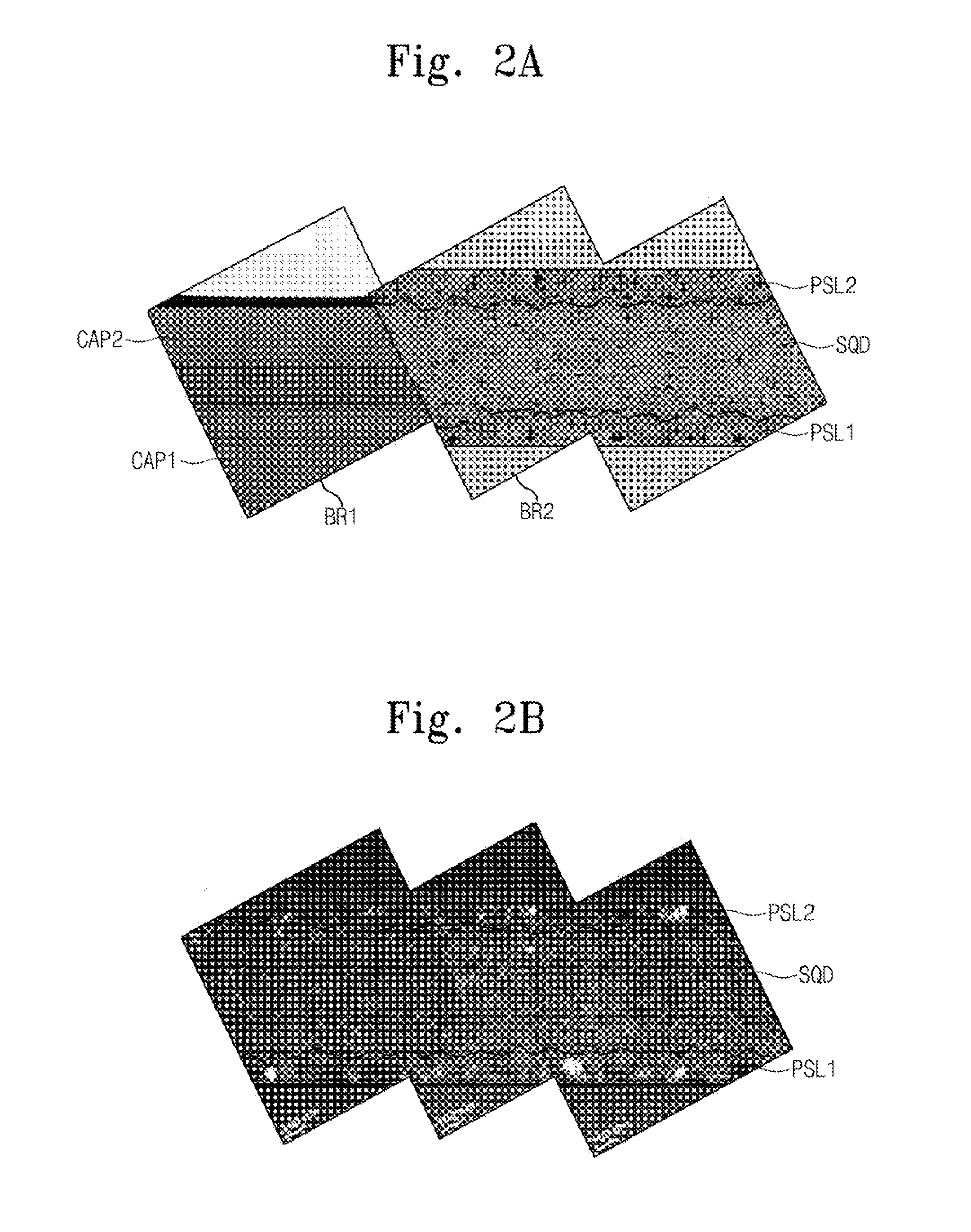
[0040]FIG. 4 is an XRD (X-ray diffraction) graph of the silicon quantum dot layer SQD formed according to the present disclosure. Referring to FIG. 4, grains of silicon quantum dots are randomly grown as 111>, 220>, and 311>.

[0041]The silicon quantum dot layer SQD fabricated through the exemplary method shown in FIGS. 2A, 2B, and 3 is applicable to various devices by using the physical characteristics of the silicon quantum dots. Each silicon quantum dot has a quantum confinement effect. The quantum confinement effect refers to a phenomenon in which the energy band gap of a material is increased if the size of a material is reduced to a Bohr exciton radius or less. Accordingly, energy corresponding to the band gap may be discharged or absorbed according to the types of quantum dots. Therefore, the silicon quantum dots are applicable to, for example, a photovoltaic conversion device, a display device, or the semiconductor layer of a thin film transistor.

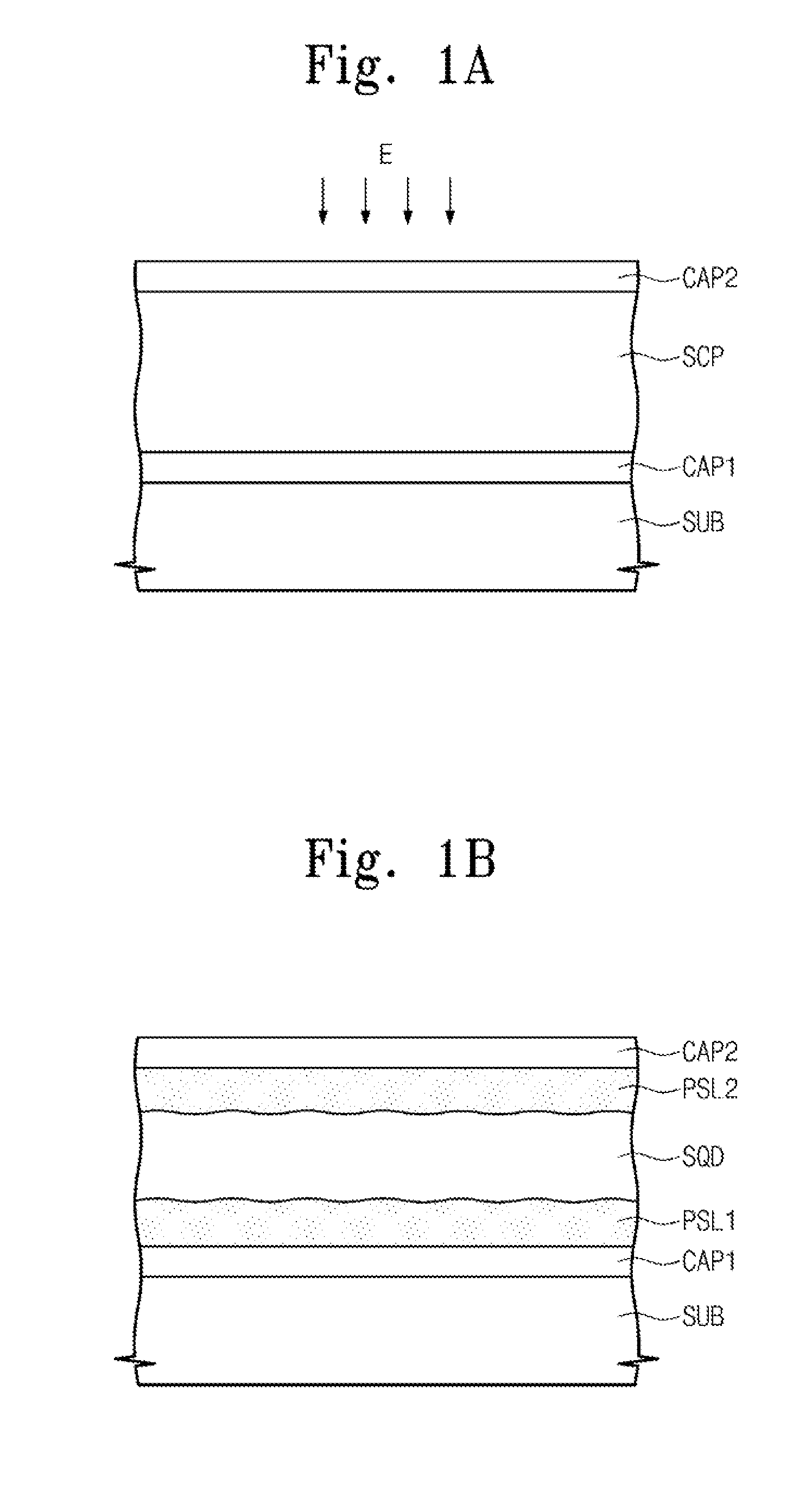
[0042]FIG. 5 is a sectional vi...

sixth embodiment

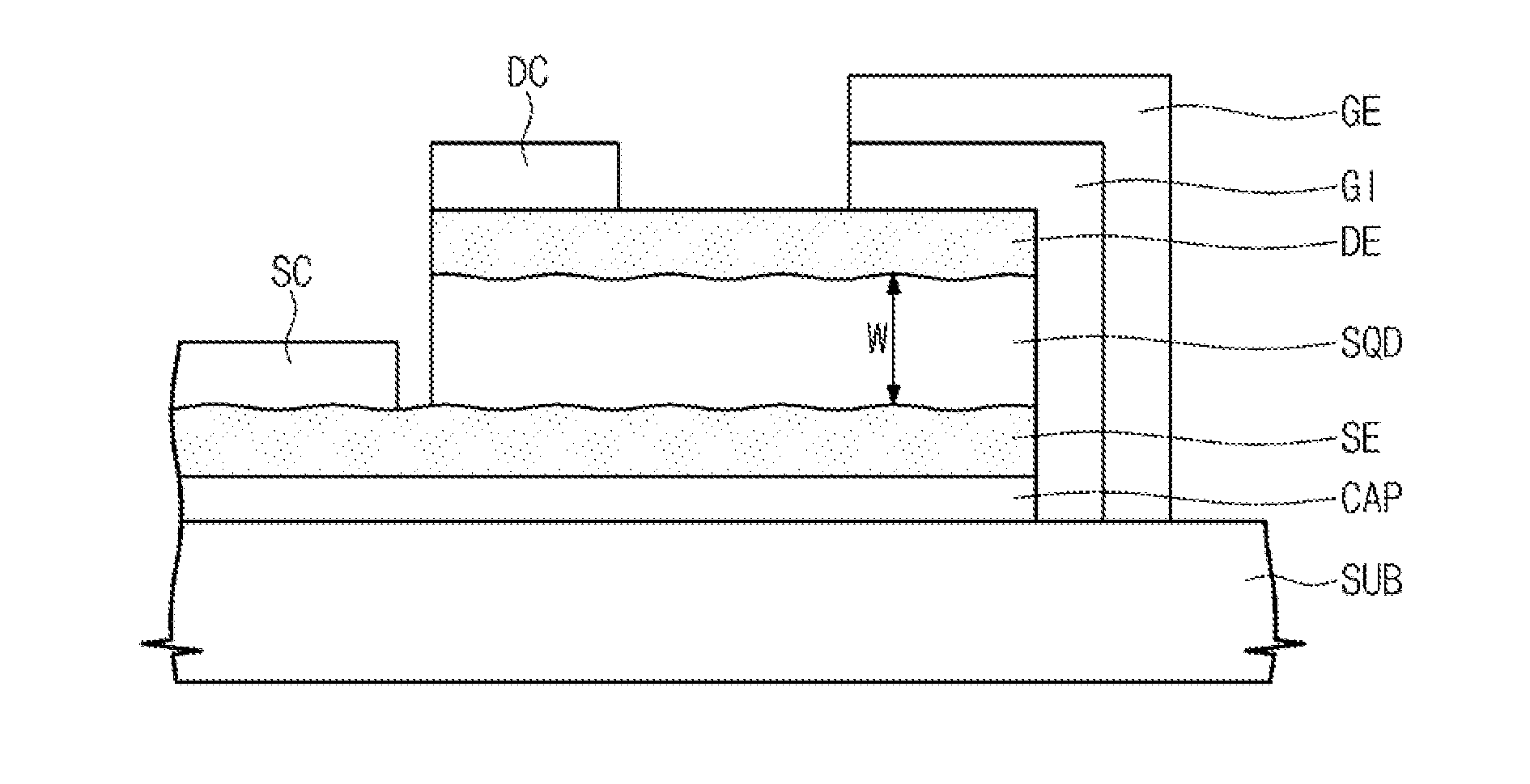
[0075]FIG. 9 is a sectional view showing a display device including the silicon quantum dot layer SQD according to a sixth exemplary embodiment of the present disclosure. The display device according to the sixth exemplary embodiment has the structure similar to that of the photovoltaic conversion device according to the second exemplary embodiment. The sixth embodiment will be described in the context of the second exemplary embodiment. Structures and components of the sixth exemplary embodiment found in of the second exemplary embodiment will not be further described. In addition, for the purpose of explanation, the same reference numbers are used in connection with the same components of the second exemplary embodiment.

[0076]The display device includes the substrate SUB having a plurality of pixel regions. The substrate SUB is provided on a plurality of light emitting devices corresponding to the pixel regions. Since the light emitting devices have the same structure, FIG. 9 show...


PUM

PropertyMeasurementUnit
thicknessaaaaaaaaaa
widthaaaaaaaaaa
conductiveaaaaaaaaaa

Abstract

Disclosed are a method of fabricating a silicon quantum dot layer and a device manufactured using the same. A first capping layer is formed on a substrate, and a silicon-containing precursor layer is formed on the first capping layer. A second capping layer is formed on the silicon-containing precursor layer. The first capping layer, the silicon-containing precursor layer, and the second capping layer are irradiated to convert the silicon-containing precursor layer into a stack including a first poly-crystalline silicon layer, a silicon quantum dot layer on the first poly-crystalline silicon layer, and a second poly-crystalline silicon layer on the silicon quantum dot layer.

Description

CROSS-REFERENCE TO RELATED APPLICATION[0001]This application relies for priority upon Korean Patent Application No. 10-2011-0005568 filed on Jan. 19, 2011, the contents of which are herein incorporated by reference in their entirety.BACKGROUND[0002]1. Technical Field[0003]The present disclosure relates to a method of fabricating a silicon quantum dot layer and a device manufactured using the same.[0004]2. Description of Related Art[0005]A photovoltaic conversion device converts light into electrical energy using a photovoltaic conversion layer. The photovoltaic conversion layer realizes a photovoltaic effect by absorbing energy of an external light and emitting free-electrons to produce a current.[0006]Typically, the photovoltaic conversion layer includes amorphous silicon. The photovoltaic conversion device including the amorphous silicon are susceptible to a photo-degradation phenomenon and a reduction in efficiency.SUMMARY[0007]According to an exemplary embodiment of the present ...

Claims


Application Information

Patent Timeline
Patent Type & Authority Applications(United States)
IPC IPC(8): H01L33/06H01L29/775H01L21/20H01L33/08B82Y40/00B82Y99/00
CPCH01L21/02488H01L21/02532H01L21/0259H01L21/02667H01L29/78642H01L31/035218Y02E10/546H01L31/03845H01L31/077H01L31/182B82Y30/00B82Y40/00H01L31/046H01L31/03682H01L31/0465Y02P70/50H01L31/04
Inventor LEE, CZANG-HOSEO, JOON-YOUNGKIM, DONG-JIN
Owner SAMSUNG DISPLAY CO LTD
Why Eureka
Try Eureka