Component and method for the manufacture thereof

a technology of components and manufacturing methods, applied in the field of components, can solve the problems of relatively expensive process control, and inability to reliably prevent molding compound, etc., and achieve the effect of cost-effective and space-saving

Inactive Publication Date: 2012-07-19
ROBERT BOSCH GMBH
View PDF3 Cites 31 Cited by
  • Summary
  • Abstract
  • Description
  • Claims
  • Application Information

AI Technical Summary

Benefits of technology

[0007]Measures are described herein which make possible a cost-effective and space-saving realization of an element package having an access channel to the membrane structure. This is achieved in that at least one further semiconductor component having at least one through hole above the MEMS element is integrated in the molding compound at a distance from the membrane structure, so that a hollow space is located between the semiconductor component and the membrane structure, and so that the access port in the molding compound opens through into the through hole of the semiconductor component and that, together with this and the hollow space between the semiconductor component and the membrane structure, forms an access channel to the membrane structure.
[0008]Departing from the side-by-side configuration of conventional pressure sensor packages, the packaging described herein is based on a stacked configuration of at least one semiconductor component over the MEMS element. A stacked configuration not only makes it possible to reduce the lateral package size, but also makes possible a realization of the access channel to the membrane structure that is reliable in terms of process, and, in fact, using standard methods of semiconductor processing, of assembly and connection technology, and molding technology, i.e., transfer molding technology.
[0010]The thus prepared semiconductor component is mounted on the top side of the MEMS element at a distance from the membrane structure. For that purpose, a common bonding material from assembly and connection technology is used, which makes it possible to fashion a hollow space between the semiconductor component and the membrane structure that is connected to the through hole.
[0012]Moreover, the component package described herein may be manufactured at low cost on multi-panel substrates, thus in a volume production. Moreover, the package design described herein makes possible a substantial decoupling of stress between the semiconductor component and the substrate. On the one hand, the distance between the semiconductor component and the substrate is relatively large. On the other hand, the semiconductor component substantially bonds only with molding compound whose thermal expansion coefficient is readily adaptable to the material of the semiconductor component. This makes it possible to largely prevent thermomechanically induced stresses in the semiconductor component and any signal drift caused by the same.
[0013]Although the semiconductor component is configured over the MEMS element, and the membrane structure protects against external influences in the manner of a cap, the lateral dimensions of the semiconductor component only need to be adapted to a limited extent to those of the MEMS element. By using a bonding layer to couple the semiconductor component and the MEMS element, lateral size differences between the semiconductor component and the MEMS element may also be readily compensated. The package design described herein makes it possible to both combine a laterally larger semiconductor component with a smaller MEMS element, as well as a smaller semiconductor component with a laterally larger MEMS element.
[0020]The semiconductor component may be integrated both face-up, as well as face-down in the molding compound of the component package according to the present invention. The semiconductor component may be configured to allow the through hole to be positioned directly over the membrane structure. However, for certain applications, it may also be advantageous for the through hole of the semiconductor component to be positioned laterally above the membrane structure, for example, to protect the membrane structure from environmental influences. Example embodiments provide for a formed filter structure to be configured in the region of the through hole in the semiconductor component to prevent dirt particles from penetrating to the membrane structure. This may be a grid-type, porous, membrane-type or foil-type structure.

Problems solved by technology

In practical applications, this method turns out to be problematic in several respects.
In the first case, the process control is relatively expensive and error-prone since the cooling of the plunger must be adapted to the plunger geometry, to the gap width between the plunger and the sensor membrane, and to the viscosity properties of the molding compound.
At any rate, in terms of process, it is not possible to reliably prevent molding compound from getting in underneath the plunger.
However, this requires a surface area allowance on the top side of the element that is otherwise not usable.
Moreover, the membranes of MEMS elements, such as microphones, for example, are often designed to be considerably thinner and more fragile than those of pressure sensor elements.
The MEMS structures in question are not performance-rated for the mechanical loads of the magnitude that occur when a molding tool is set down sealingly.
Accordingly, integrating an ASIC in the microphone package inevitably leads to an enlarged package surface area.
Along with the package surface area, the manufacturing costs also increase, making microphone packages of this kind relatively expensive.

Method used


Image

  • Component and method for the manufacture thereof
  • Component and method for the manufacture thereof
  • Component and method for the manufacture thereof

Examples


Embodiment Construction

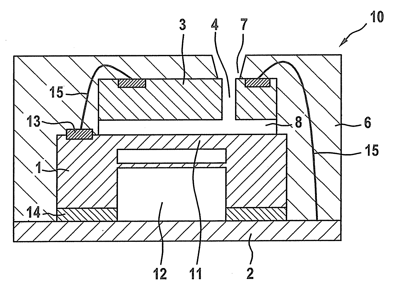
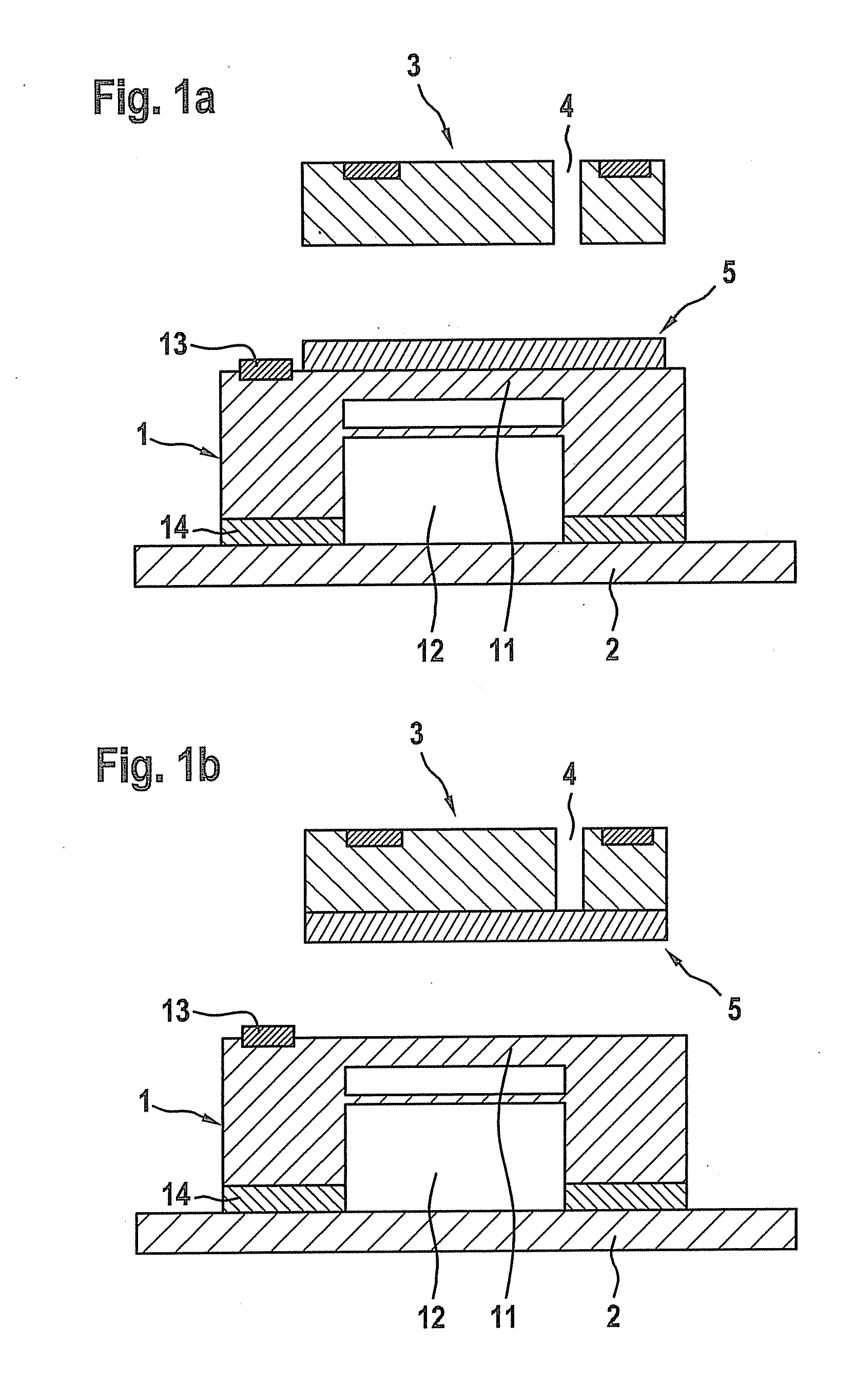
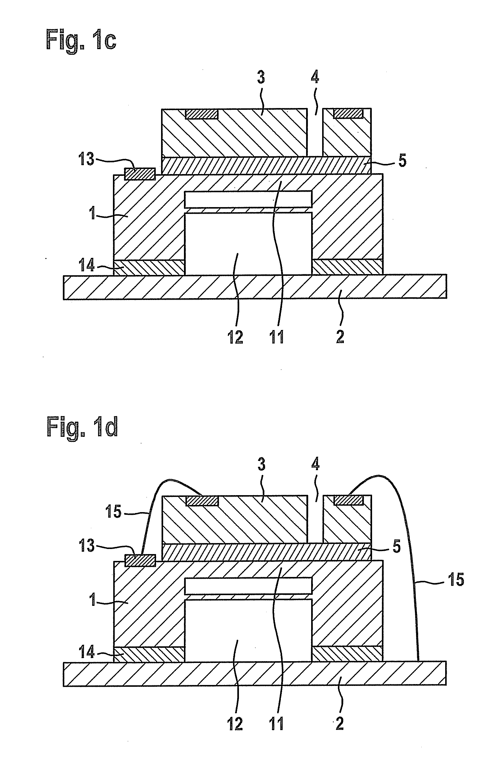
[0028]FIGS. 1a to 1b illustrate an MEMS microphone element 1 in whose top side a membrane structure 11 having signal acquisition device is configured. These may be contacted via a terminal pad 13 on the top side of microphone element 1. Membrane structure 11 spans a cavity 12 in the rear side of the element. Microphone element 1 is mounted by its rear component side on a planar substrate 2, so that the rear-side volume of microphone element 1 is bounded by cavity 12, together with substrate 2. Acoustic ports to the rear side volume may also be configured in the membrane structure. In this case, a circuit board substrate, on which microphone element 1 has been fixed in position with the aid of adhesive 14, is used as substrate 2. The circuit board substrate is advantageously a multi-panel substrate.

[0029]Illustrated above microphone element 1 in each case is an ASIC 3 having a through hole 4 that is to be configured on microphone element 1 and with clearance from membrane structure 1...


PUM


Abstract

A cost-effective and space-saving component that includes a MEMS element and an access channel to the membrane structure of the MEMS element.The MEMS element is mounted by the rear side of the component on a substrate and is at least partially embedded in a molding compound. An access port is formed in the molding compound. The component also includes at least one semiconductor component having at least one through hole that is integrated in the molding compound above the MEMS element at a distance from the membrane structure, so that a hollow space is located between the semiconductor component and the membrane structure. The access port in the molding compound opens into the through hole of the semiconductor component and, together with this and the hollow space between the further semiconductor component and the membrane structure, forms the access channel to the membrane structure.A cost-effective and space-saving component that includes a MEMS element and an access channel to the membrane structure of the MEMS element. The MEMS element is mounted by the rear side of the component on a substrate and is at least partially embedded in a molding compound. An access port is formed in the molding compound. The component also includes at least one semiconductor component having at least one through hole that is integrated in the molding compound above the MEMS element at a distance from the membrane structure, so that a hollow space is located between the semiconductor component and the membrane structure. The access port in the molding compound opens through into the through hole of the semiconductor component and, together with this and the hollow space between the further semiconductor component and the membrane structure, forms the access channel to the membrane structure.

Description

CROSS-REFERENCE TO RELATED APPLICATIONS[0001]The present application claims priority to Application No. 10 2010 064 120.0, filed in the Federal Republic of Germany on Dec. 23, 2010, which is expressly incorporated herein in its entirety by reference thereto.FIELD OF THE INVENTION[0002]The present invention relates to a component, as well as to a method for the manufacture thereof. For example, the component includes at least one MEMS element having at least one membrane structure configured in the top side thereof. The MEMS element is mounted by the rear side thereof on a substrate. Moreover, the MEMS element is at least partially embedded in a molding compound in which at least one access port is formed.BACKGROUND INFORMATION[0003]German Published Patent Application No. 199 29 026 describes using a molded housing for packaging an MEMS pressure sensor element. A sensor membrane, which spans a cavity in the rear side of the element, is configured in the top side of the pressure senso...

Claims


Application Information

Patent Timeline
Patent Type & Authority Applications(United States)
IPC IPC(8): H01L29/84H01L21/02
CPCB81B7/0061B81B2201/0257B81C2203/0154H04R19/04H04R31/00H04R19/005H01L2224/32145H01L2224/48091H01L2224/73265H01L2924/00014
Inventor EHRENPFORDT, RICARDOSCHOLZ, ULRIKE
Owner ROBERT BOSCH GMBH
Why Eureka
Try Eureka