Method of manufacturing a package for embedding one or more electronic components

a technology for electronic components and carrier structures, applied in the incorporation of printed electric components, semiconductor/solid-state devices, printed circuit aspects, etc., can solve problems such as disturbance of guided wave modes, chip analog front-ends or multi-channel chips, and lossy connection of chip-to-chip connections, so as to accelerate the development of such electronic systems

Active Publication Date: 2012-07-19
SONY CORP
View PDF10 Cites 41 Cited by
  • Summary
  • Abstract
  • Description
  • Claims
  • Application Information

AI Technical Summary

Benefits of technology

[0013]It is an object of the present invention to provide a method of manufacturing a carrier structure of a package for embedding one or more electronic components and to a method of manufacturing a package by which the above explained disadvantages are prevented.
[0014]It is a further object of the present invention to provide a carrier structure of a package for embedding one or more electronic components, an electronic component for being embedded in a carrier structure and to a package by which the above explained disadvantages are prevented.
[0042]The proposed approach leads to functional blocks that are electromagnetically completely shielded. These units can be combined and cascaded according to system needs. The danger is minimized that unwanted resonant modes inside the package are excited which cause system failures hard to debug. The functional blocks once characterized properly can be used in system simulations to investigate arbitrary system architectures. Rapid translation of system level designs into a real package will become possible and may accelerate the development of such electronic systems.

Problems solved by technology

These and other known methods for manufacturing a package for embedding one or more electronic components, in particular microwave integrated circuits and discrete passive components, and methods for manufacturing electronic systems show various problems or disadvantages.
At THz frequencies chip-to-chip connections become very lossy and single-chip analog front-ends or multi-channel chips will likely be encountered with sizes larger than λ0.
At chip interconnections guided wave modes get disturbed.
Dielectric losses of packaging materials increase with frequency.
Thus, the full embedding of MMICs in dielectric material is practically not attractive anymore at mm-wave / THz frequencies but is done at lower frequencies.
The photolithographically structured features on the front side of the MMIC become very small and little area is available for lid attachment on the chip.
MMICs are often thin and fragile, and mechanical attachment to the lid is difficult, e.g. using a flip-chip approach.
They are often difficult to design and their ability to suppress cavity modes is band-limited.
In addition small manufacturing changes may shift the suppression band.
Packaging of wideband systems is challenging.
Their size is large compared to the wavelength and integration of such components into the package may either alter the original filter characteristic or disturb other functional blocks of the system due to modal coupling into spurious package modes.
Many packaging approaches at mm-wave and THz frequencies cannot be decomposed into electromagnetically separated units.
Multichip packages are difficult to design and hard to debug due to the complex electromagnetic situation inside the package.
This leads to long design cycles.
Alternatively each functional block requires a separate package which leads to the problem of interconnecting these packages at mm-wave / THz frequencies.
The so called split block technology is commonly in use in these scenarios which may lead to bulky and expensive electronic systems.

Method used


Image

  • Method of manufacturing a package for embedding one or more electronic components
  • Method of manufacturing a package for embedding one or more electronic components
  • Method of manufacturing a package for embedding one or more electronic components

Examples


Embodiment Construction

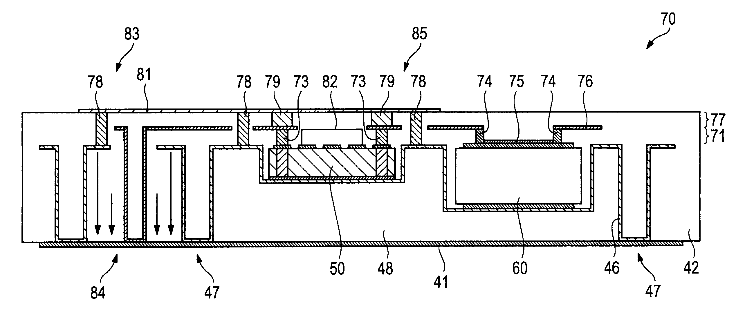
[0060]The present invention makes use of a method of manufacturing by which packages for embedding one or more electronic components, in particular microwave integrated circuits and discrete passive components (e.g. capacitors or resistors), are more or less cast from a single piece of material. The final package is in that sense a kind of monolithic package. The package material is preferably a light sensitive monomer that is steadily poured into place in thin layers and hardened by photo polymerization using light at UV or other wavelengths.

[0061]Such methods have become available in recent years for manufacturing of microparts and are used for integrating chips at lower frequencies, i.e. frequencies much below the microwave spectrum. Micrometer precision in vertical and lateral dimensions is possible. Common materials belong to the group of acrylics. However, these materials often exhibit high dielectric losses which are not very attractive for multichip packages at mm-wave / THz f...


PUM

PropertyMeasurementUnit
Widthaaaaaaaaaa
Thicknessaaaaaaaaaa
Electrical conductoraaaaaaaaaa

Abstract

The present invention relates to the field of integrating electronic systems that operate at mm-wave and THz frequencies. A monolithic multichip package, a carrier structure for such a package as well as manufacturing methods for manufacturing such a package and such a carrier structure are proposed to obtain a package that fully shields different functions of the mm-wave / THz system. The package is poured into place by polymerizing photo sensitive monomers. It gradually grows around and above the MMICs (Monolithically Microwave Integrated Circuit) making connection to the MMICs but recessing the high frequency areas of the chip. The proposed approach leads to functional blocks that are electromagnetically completely shielded. These units can be combined and cascaded according to system needs.

Description

CROSS-REFERENCE TO RELATED APPLICATIONS[0001]The present application claims priority of European patent application 11151208.3 filed on Jan. 18, 2011.FIELD OF THE INVENTION[0002]The present invention relates to a method of manufacturing a carrier structure of a package for embedding one or more electronic components, in particular microwave integrated circuits and discrete passive components, and to a method of manufacturing a package comprising one or more electronic components.[0003]Further, the present invention relates to a carrier structure of a package for embedding one or more electronic components, in particular microwave integrated circuits and discrete passive components, to an electronic component for being embedded in a carrier structure of a package and to a package comprising such a carrier structure and one or more electronic system embedded therein.BACKGROUND OF THE INVENTION[0004]WO 2004 / 070835 A1 discloses a method for producing microsystems comprising microelectro...

Claims


Application Information

Patent Timeline
IPC IPC(8): H01L25/00H05K1/02H05K13/00H01L21/56
CPCH05K1/0243H05K1/16H01L2924/0002H05K1/185H05K2201/0715H05K2201/0723H05K2201/09972H05K2203/1469H01L25/16H01L2223/6616H01L2223/6633H01L2223/6677H01L2223/6683H01L23/66H05K2201/09981H01L23/49827H01L23/5389H01L2924/00H01L2924/19105H01L23/64H05K3/301H05K3/465H05K3/4697
Inventor MERKLE, THOMASKOCH, STEFANCHOI, JOO-YOUNG
Owner SONY CORP
Why Eureka
Try Eureka