Check patentability & draft patents in minutes with Patsnap Eureka AI!

Three-Dimensional Stacked and-Type Flash Memory Structure and Methods of Manufacturing and Operating the Same Hydride

a flash memory structure and three-dimensional stacking technology, applied in the field of three-dimensional stacked and-type flash memory structure and manufacturing and operating the same, can solve the problems of time-consuming and expansive, and the expansive cost limit the staked layers of the 3d flash memory structure, and achieve the effect of improving read latency

Active Publication Date: 2012-07-19
MACRONIX INT CO LTD
View PDF1 Cites 30 Cited by
  • Summary
  • Abstract
  • Description
  • Claims
  • Application Information

AI Technical Summary

Benefits of technology

The patent describes a 3D stacked AND-type flash memory structure and a method of manufacturing it. The structure includes several horizontal planes of memory cells arranged in a three-dimensional array, with each horizontal plane comprising several word lines and several charge trapping multilayers alternately arranged. The structure also includes a plurality of sets of bit lines and source lines arranged alternately and disposed vertically to the horizontal planes, and a plurality of sets of channels and insulation pillars arranged alternatively and disposed perpendicularly to the horizontal planes. The structure is suitable for one-bit per cell operation and two-bit per cell operation. The method of manufacturing involves depositing layers of insulation and patterning them to form WL stacks and trenches between them. A conductive layer is then deposited to fill the trenches and patterned to form BL stacks. The structure is designed to improve read latency and provide faster access to memory cells.

Problems solved by technology

However, the processes for manufacturing those three-dimensional NAND-type flash memory structures require several critical lithography steps for each memory layer, which is time-consuming and expansive.
Although the benefits of higher density are achieved using 3D arrays, the expansive costs limit the staked layers of the 3D flash memory structures.

Method used


Image

  • Three-Dimensional Stacked and-Type Flash Memory Structure and Methods of Manufacturing and Operating the Same Hydride
  • Three-Dimensional Stacked and-Type Flash Memory Structure and Methods of Manufacturing and Operating the Same Hydride
  • Three-Dimensional Stacked and-Type Flash Memory Structure and Methods of Manufacturing and Operating the Same Hydride

Examples


Embodiment Construction

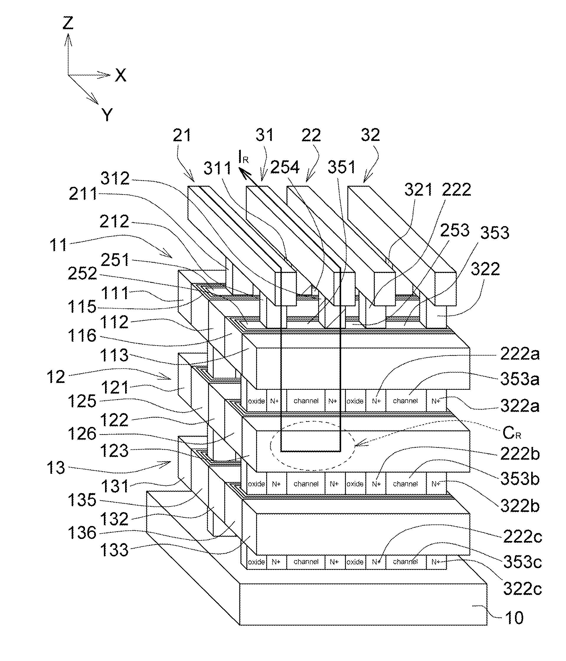
[0029]In the embodiment of the present disclosure, a 3D stacked AND-type flash memory structure and method of manufacturing the same are provided. Also, related operation methods such as reading, programming and erasing the 3D stacked AND-type flash memory structure of the embodiment are also described herein. The MOSFET (Metal-Oxide-Semiconductor Field-Effect Transistor) of the 3D stacked AND-type flash memory structure are parallelly connected instead of serially connected in the NAND-type flash memory structure; thus, the read latency can be greatly enhanced. Also, the 3D stacked AND-type flash memory structure of the embodiment can be programmed by channel hot electron programming (CHE) method like NOR Flash, or programmed by FN (Fowler-Nordheim) tunneling method like NAND Flash. In the embodiment of the present disclosure, the device is a double-gated charge-trapping device, and the double gates could be independently decoded, so that physically two bit / cell operation can be ca...


PUM


Abstract

A 3D stacked AND-type flash memory structure comprises several horizontal planes of memory cells arranged in a three-dimensional array, and each horizontal plane comprising several word lines and several of charge trapping multilayers arranged alternately, and the adjacent word lines spaced apart from each other with each charge trapping multilayer interposed between; a plurality of sets of bit lines and source lines arranged alternately and disposed vertically to the horizontal planes; and a plurality of sets of channels and sets of insulation pillars arranged alternatively, and disposed perpendicularly to the horizontal planes, wherein one set of channels is sandwiched between the adjacent sets of bit lines and source lines.

Description

BACKGROUND[0001]1. Field of the Invention[0002]The disclosure relates in general to a three-dimensional (3D) flash memory structure and methods of manufacturing and operating the same, and more particularly to a 3D stacked AND-type flash memory structure and methods of manufacturing and operating the same.[0003]2. Description of the Related Art[0004]A nonvolatile semiconductor memory device is typically designed to securely hold data even when power is lost or removed from the memory device. Various types of nonvolatile memory devices have been proposed in the related art. Also, manufactures have been looking for new developments or techniques combination for stacking multiple planes of memory cells, so as to achieve greater storage capacity. For example, several types of multi-layer stackable thin-film transistor (TFT) NAND-type flash memory structures have been proposed.[0005]However, the processes for manufacturing those three-dimensional NAND-type flash memory structures require...

Claims


Application Information

Patent Timeline
Patent Type & Authority Applications(United States)
IPC IPC(8): G11C11/34H01L21/336H01L29/792
CPCH01L27/11524G11C16/0416G11C8/16H01L27/11556H10B41/35H10B41/27
Inventor LUE, HANG-TING
Owner MACRONIX INT CO LTD
Features
  • R&D
  • Intellectual Property
  • Life Sciences
  • Materials
  • Tech Scout
  • Unparalleled Data Quality
  • Higher Quality Content
  • 60% Fewer Hallucinations
Learn More