
Patsnap Eureka
For R&D, Patsnap Eureka makes reading and utilizing patents & technical documents easy.
Patsnap Eureka AIR
Designed for self-driven R&D workflows. Generate viable solutions, solve complex R&D challenges, empower your innovation with AI.

Patsnap Eureka Materials
Designed for material experts only. Revolutionize your material R&D, from search, analyze, to developing new materials.

TechResearch
Generate reliable direction feasibility study reports for your R&D in just a few steps.

TechSeek
Discover and master advanced knowledge NOW. Basics, ideas, possibilities, all at once.

TechMind
As an expert in R&D Theories, TechMind can generates customized viable solutions instantly.

TechRisk
Analyze your overall solution with one click, know your potential R&D risks in advance.

TechMonitor
Get weekly tech updates, stay abreast of the latest tech innovations and key insights.
Device and method for boron diffusion in semiconductors
a technology of boron diffusion and semiconductors, applied in the field of semiconductor fabrication, can solve the problems of ion implantation introducing crystal damage, displacement of lattice silicon atoms, and severe drawbacks of each of the above mentioned boron doping methods
- Summary
- Abstract
- Description
- Claims
- Application Information
AI Technical Summary
Problems solved by technology
Method used
Image

Examples
Embodiment Construction
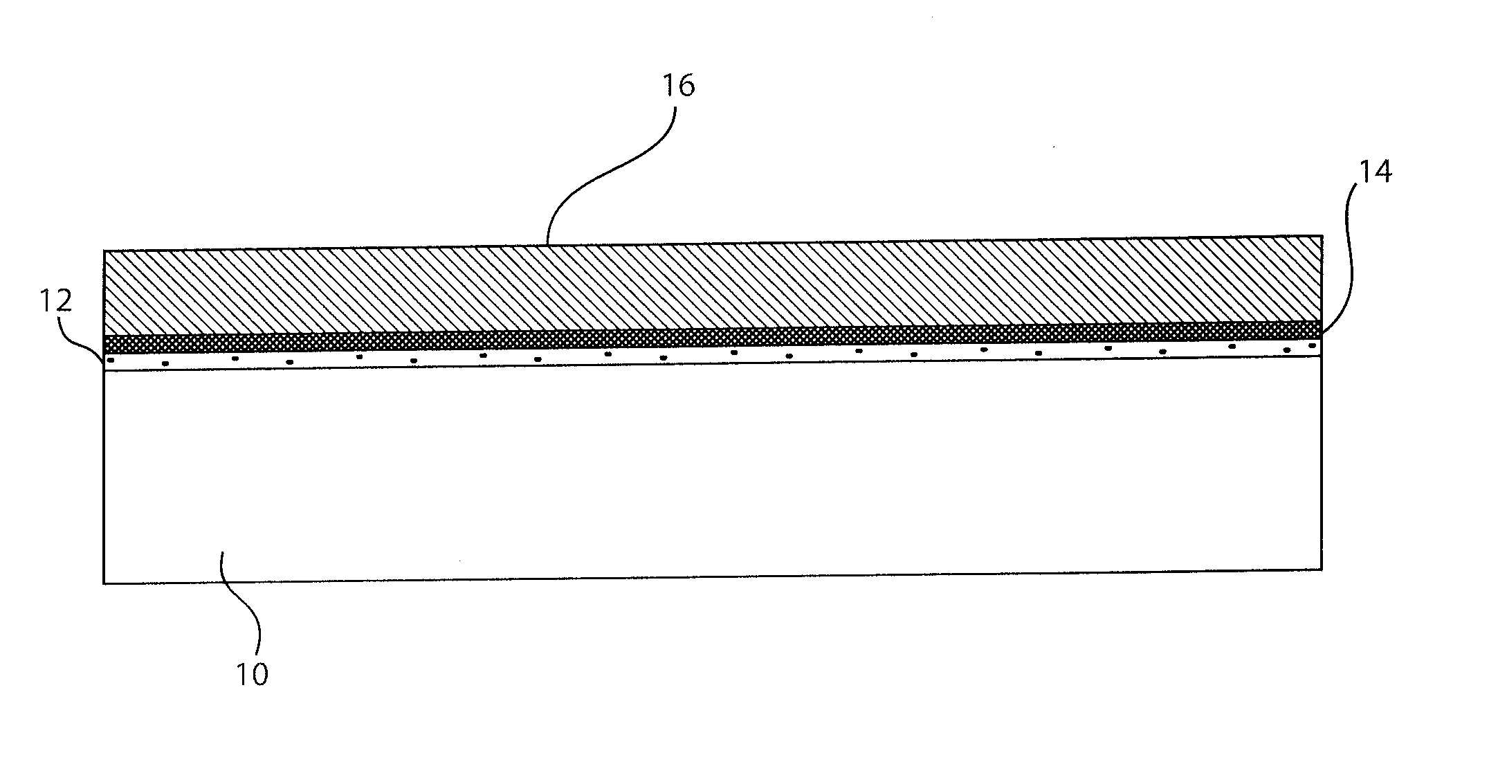
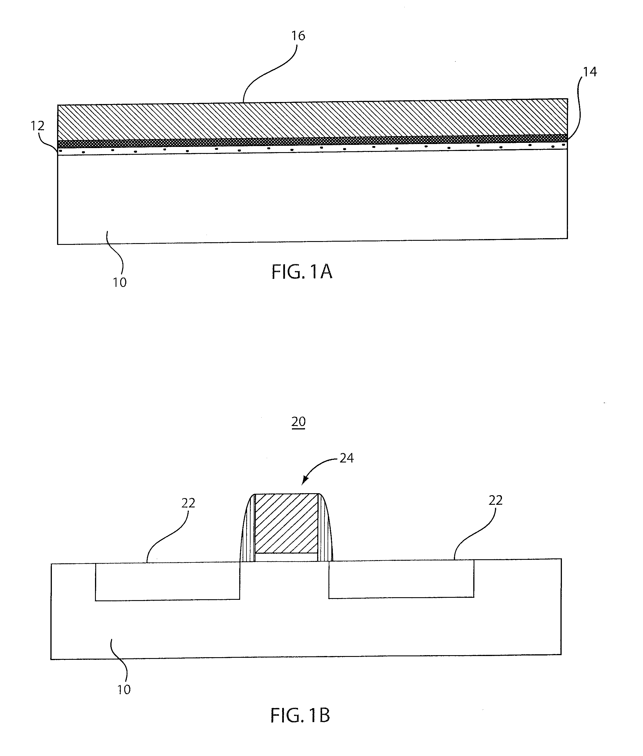
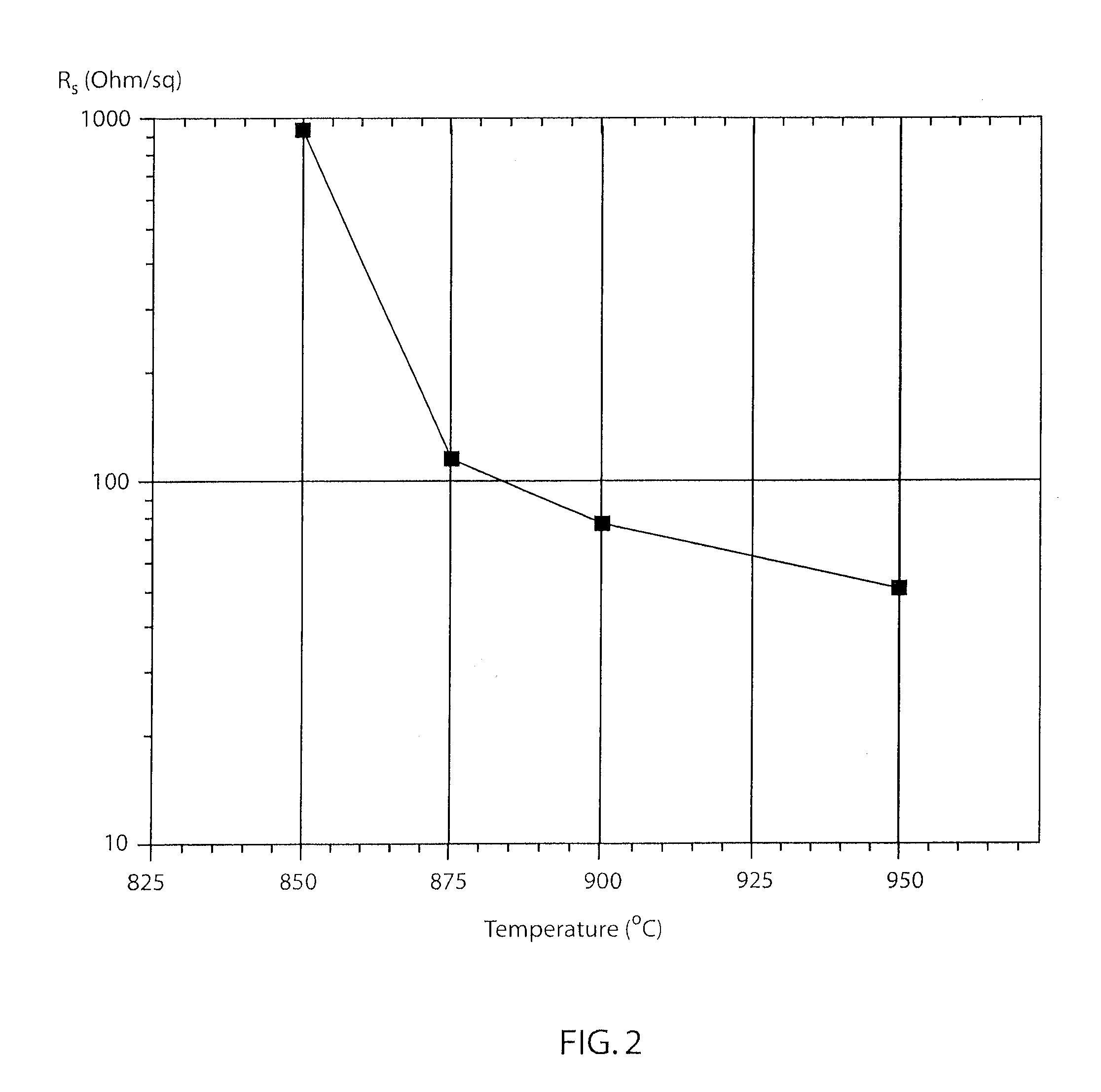
[0021]The present principles provide methods for low cost Boron doping that prevents the formation of a Boron Rich Layer (BRL) e.g., a SiB6 phase. The methods provide a low cost device that does not suffer from the drawbacks of conventional devices. An amorphous or polyscrystalline elemental layer, e.g., including Boron, is formed on a buffer layer which is in turn formed on a semiconductor material. Boron atoms from the layer are diffused into the buffer layer and then into the semiconductor. A supply of Boron atoms to the semiconductor is limited by the diffusivity in the buffer layer.
[0022]In one embodiment, the diffusivity of the atoms in the buffer layer may be selected to be less than the diffusivity of atoms in the semiconductor, and a segregation coefficient of the atoms at the buffer layer / semiconductor interface may be selected to be lower than 1. In this way, cost effective dopant diffusion may be provided with a high concentration of surface atoms and without the formati...
PUM
 Abstract
Description
Claims
Application Information
 - R&D Engineer
- R&D Manager
- IP Professional
- Industry Leading Data Capabilities
- Powerful AI technology
- Patent DNA Extraction
Browse by: Latest US Patents, China's latest patents, Technical Efficacy Thesaurus, Application Domain, Technology Topic, Popular Technical Reports.
© 2024 PatSnap. All rights reserved.Legal|Privacy policy|Modern Slavery Act Transparency Statement|Sitemap|About US| Contact US: help@patsnap.com