
Injection molding system and method of chip package

a technology which is applied in the field of injection molding system and chip package injection molding, can solve the problems of consuming time and cost, complicated production process of conventional chip package, etc., and achieve the effect of reducing the cost and time of chip package production, shortening the process, and effectively reducing the time of package production

Active Publication Date: 2012-07-26
ADL ENG
View PDF6 Cites 8 Cited by
  • Summary
  • Abstract
  • Description
  • Claims
  • Application Information

AI Technical Summary

Benefits of technology

[0009]One object of the present invention is to reduce the cost and time of production of a chip package. The present invention provides an injection molding system and method thereof to shorten the process and reduce the time of package production effectively.
[0010]Another object of the present invention is to improve the stability of the package structure. The structure provided in the present invention is more stable than the conventional structure, which utilizes the addition of an inner cover before forming the filling layer.
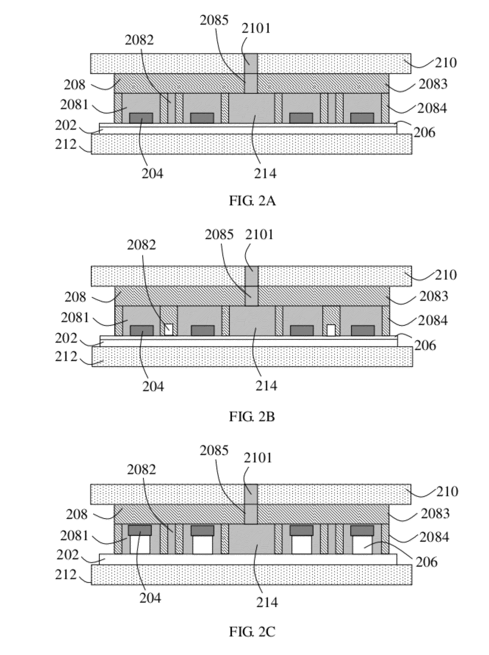
[0011]For achieving the objects mentioned above, one embodiment of the present invention provides an injection molding system for a semiconductor package to predigest (i.e., simplify) the package process and reduce the cost, such as time, manpower or finance. The injection molding system comprises a substrate for locating at least one semiconductor device under molding, an inner cover with at least one first injection via, cavity and runner placed over the substrate for covering the semiconductor device under molding, a molding tool with at least one second injecting via aligned with the first injection via of the inner cover, and a bottom plate placed under the substrate. Furthermore, a filling material is filled into the cavity and runner of the inner cover during molding. In order to avoid the filling material overflowing, the system further comprises an O-ring placed between the molding tool and the inner cover. The inner radius of the O-ring corresponds with the inner radius of the first injection or second injection and aligned with those.
[0012]In one embodiment, the inner cover is defined by a top plate and a plurality of pillars arranged under the bottom of the top plate. Each pair of the pillars is placed by both sides of each semiconductor device. The first injection is configured on the top plate. The bottom plate further includes heat-function members, such as a heater or a heating plate to thermoform the filling material, if it is needed. The second adhesion layer is formed on the semiconductor device, which could be a conductive material, a non-conductive material or a thermoplastic material. The second adhesion layer fixes the inner cover and enhances the heat dissipation. The molding tool further includes checking windows to check a status of the filling material, like whether the filling material is overflowed when injecting the filling material.
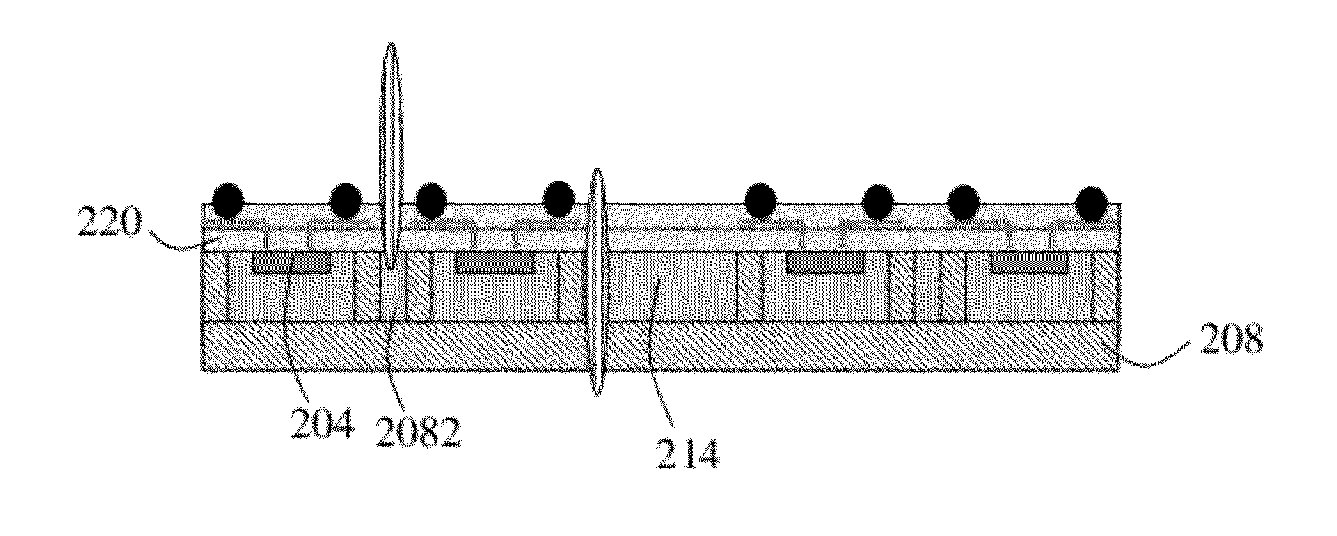
[0014]Therefore, the semiconductor device or chip has embedded in the substrate by this injection molding system. Because this injection molding system is easy to use and which integrates two or more steps of a conventional package process, the package process would be effectively predigested (i.e., simplified). In other words, the present system effectively predigests the package process and reduces the cost of the package process. Then, at least one redistribution layer is formed over the semiconductor device, the filling material and the inner cover in a continuous step.

Problems solved by technology

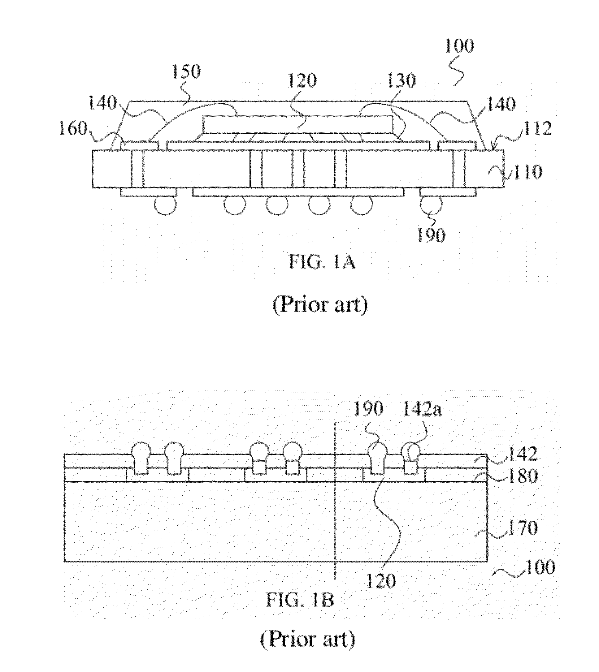
However, the production of the conventional chip package has a complicated process and consumes much time and cost.

Method used


Image

  • Injection molding system and method of chip package
  • Injection molding system and method of chip package
  • Injection molding system and method of chip package

Examples


Embodiment Construction

[0025]The detailed description provided below in connection with the appended drawings is intended as a description of the preferred embodiments and is not intended to represent the only forms in which the present embodiments may be constructed or utilized. The description sets forth the functions of the example and the sequence of steps for constructing and operating the embodiments. However, the same or equivalent functions and sequences may be accomplished by different examples.

[0026]In accordance with common practice, the various described elements are not drawn to scale but are drawn to illustrate specific elements relevant to the present invention. Like reference numbers and designations in the various drawings indicate like elements.

[0027]The present invention discloses an injection molding system for a semiconductor package and the method thereof to improve the performance of packaging structure and reduce the cost of manufacture. In order to predigest the package process fo...


PUM

PropertyMeasurementUnit
pressureaaaaaaaaaa
adhesionaaaaaaaaaa
structureaaaaaaaaaa

Abstract

The injection molding system comprises a substrate, an inner cover, a molding tool, and a bottom plate. The substrate is used to locate at least one semiconductor device under molding and the inner cover with at least one first injection via, cavity and runner placed over the substrate. In addition, the molding tool includes at least one second injecting via aligned with the runner and the bottom plate is placed under the substrate. Furthermore, a filling material is filled into the cavity and runner of the inner cover during molding. In order to avoid overflowing the filling material, the system further comprises an O-ring placed between the molding tool and the inner cover. The inner radius of the O-ring corresponds with the inner radius of the injection via and is aligned with it.

Description

FIELD OF THE INVENTION[0001]The present invention relates to a chip package. More particularly, the present invention relates to an injection molding system and method for injection molding of a chip package to improve the performance of packaging structure and reduce the cost of manufacture.BACKGROUND OF THE INVENTION[0002]In semiconductor industries, the production of integrated circuits (ICs) mainly includes three steps: manufacturing a wafer, manufacturing integrated circuits and packaging the integrated circuits. A bare chip is formed after the steps of wafer manufacturing, circuit designing, mask manufacturing and wafer dicing. Each bare chip formed from dicing the wafer is electrically connected to an external signal through connecting points on each bare chip, and then the bare chip is encapsulated by a molding material. The purpose of the package is to prevent the bare chip from being damaged by humidity, heat and noise signals, and to provide the bare chip with an electric...

Claims


Application Information

Patent Timeline
Patent Type & Authority Applications(United States)
IPC IPC(8): H01L23/28B29C45/14H01L21/56
CPCB29C45/14639H01L21/565H01L23/3121H01L24/19H01L2224/0401H01L24/97H01L2224/04105H01L2224/12105H01L24/96H01L2924/15788H01L2924/181H01L2924/14H01L2223/6677H01L2924/00
Inventor CHEN, WEN-CHUANLIN, NAN-CHUN
Owner ADL ENG
Learn More