Communication device and antenna structure therein

Active Publication Date: 2012-07-26
ACER INC
View PDF2 Cites 13 Cited by
  • Summary
  • Abstract
  • Description
  • Claims
  • Application Information

AI Technical Summary

Benefits of technology

[0010]In an embodiment of the invention, the length of the antenna element is only about 45 mm, wherein two ends of the antenna element extend away from each other. A ground element and the corresponding edge of the antenna element form a current path that is similar to a loop antenna. This makes the length of the antenna element become much smaller than the resonant length of a traditional loop antenna with its two ends close to each other. With respect to the antenna element of the invention, a 900-MHz band is excited by an additional capacitive element, and an 1800-MHz band is excited by an additional inductive element. Also, the additional inductive element is configured to adjust the impedance matching of the 900-MHz band. In other embodiments, a matching circuit may be incorporated to adjust the impedance matching of th

Problems solved by technology

Since the space in mobile communication devices is limited, it is required that an antenna designer consider the performan

Method used


Image

  • Communication device and antenna structure therein
  • Communication device and antenna structure therein
  • Communication device and antenna structure therein

Examples


first embodiment

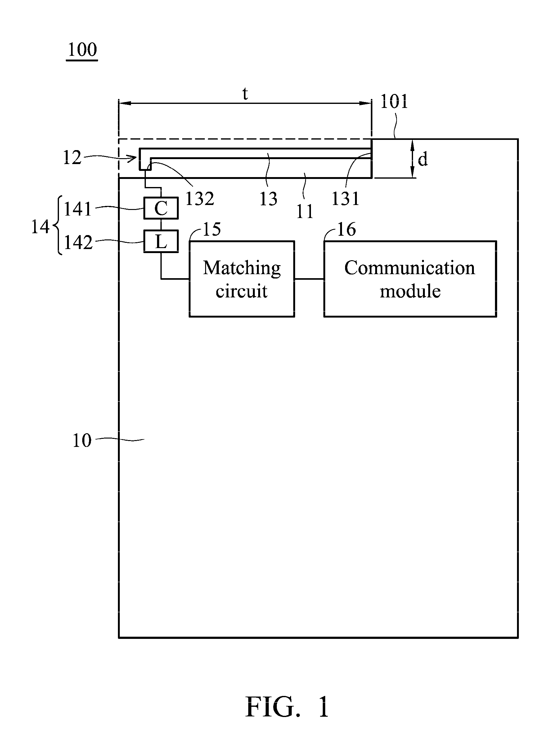
[0019]FIG. 1 is a diagram for illustrating a communication device 100 and an antenna structure therein according to the invention. The communication device 100 comprises an antenna structure. The antenna structure comprises a ground element 10, an antenna element 12, and a circuit element group 14. An edge 101 of the ground element 10 has a notch 11, wherein a long edge t of the notch 11 is at least two times longer than a short edge d of the notch 11. The antenna element 12 comprises a metal portion 13 disposed in the notch 11. Two ends 131 and 132 of the metal portion 13 extend away from each other and are positioned substantially at or around two opposite edges of the notch 11, wherein the end 131 is electrically coupled to the ground element 10, and the other end 132 is a feeding terminal of the antenna element 12. The circuit element group 14 comprises at least a capacitive element 141 and an inductive element 142. The capacitive element 141 and the inductive element 142 are co...

second embodiment

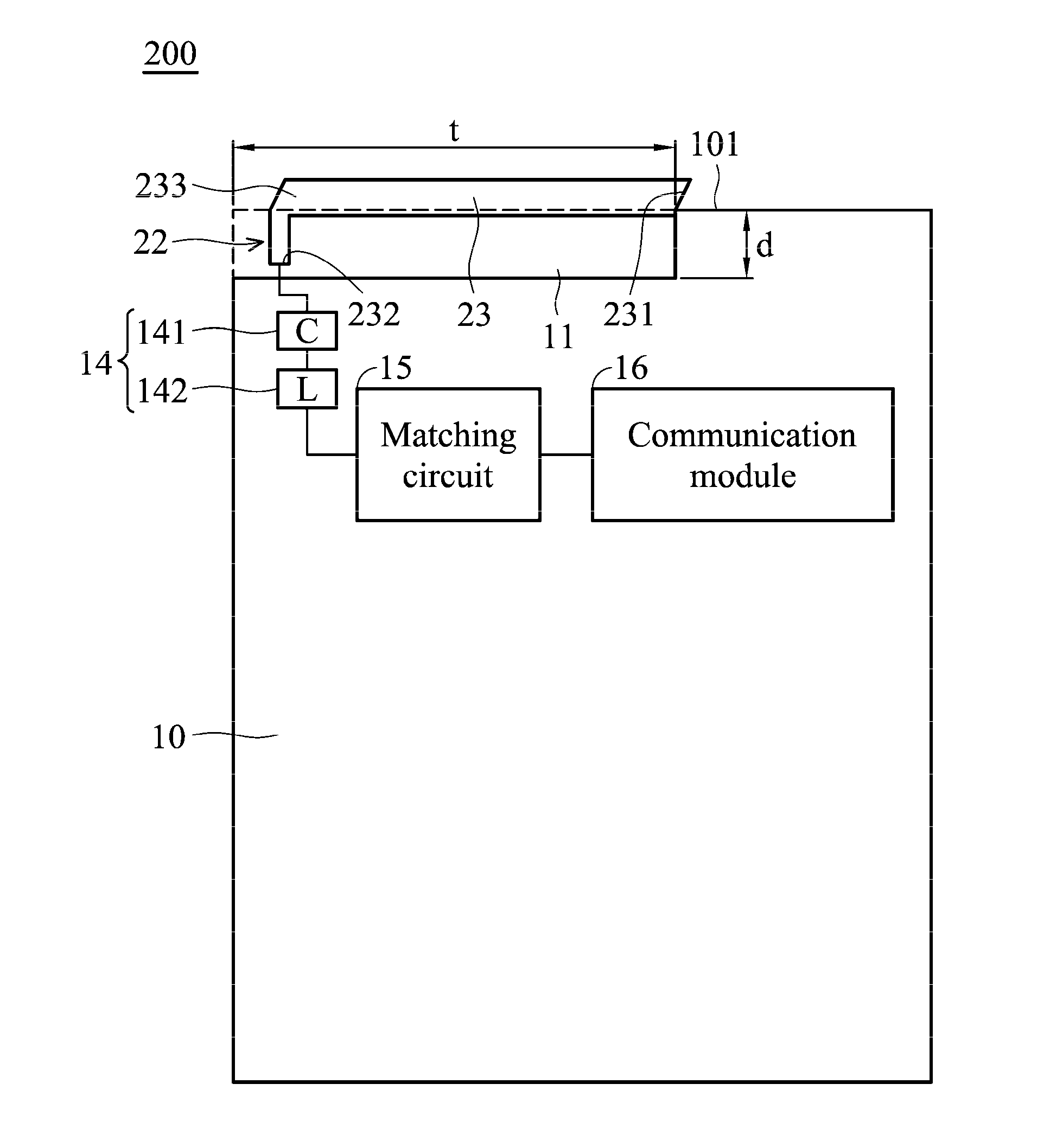
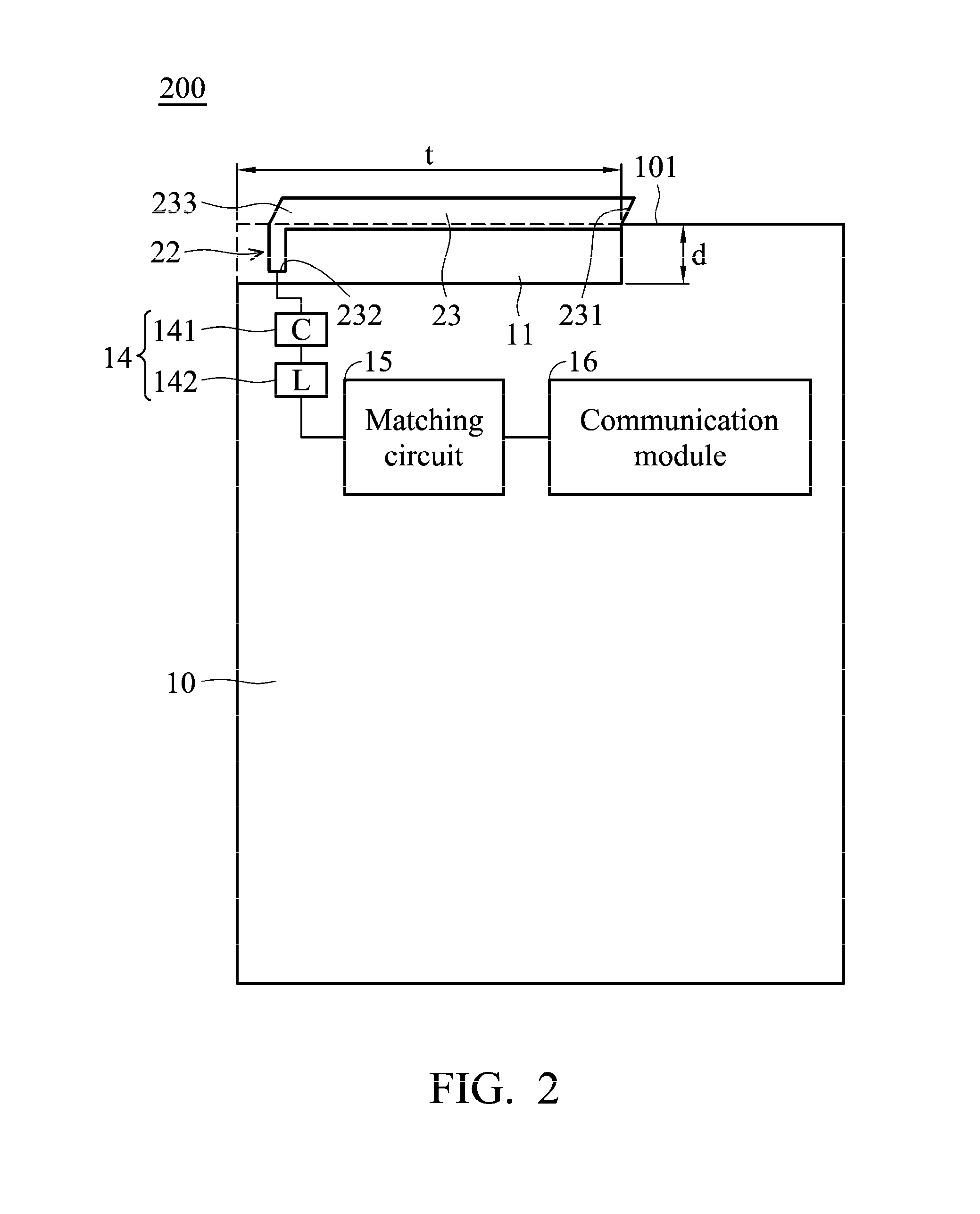
[0022]FIG. 4 is a diagram for illustrating antenna efficiency of the communication device 200 and the antenna structure therein according to the invention, wherein the vertical axis represents the antenna efficiency (%), and two horizontal axes represent an operating frequency (unit: MHz). The antenna efficiency curve 41 corresponds to the lower horizontal axis, and the antenna efficiency curve 42 corresponds to the upper horizontal axis. The antenna efficiency curve 41 represents antenna efficiency of the antenna structure in a GSM900 band (880 MHz˜960 MHz), and the antenna efficiency curve 42 represents antenna efficiency of the antenna structure in a GSM1800 band (1710 MHz˜1880 MHz). The communication device and the antenna structure of the invention have good antenna efficiency (the return loss included in the antenna efficiency) in the GSM900 and GSM1800 bands to meet practical applications.

[0023]FIG. 5 is a diagram for illustrating a communication device 500 and an antenna str...


PUM


Abstract

A communication device including an antenna structure is provided, wherein the antenna structure includes a ground element, an antenna element, and a circuit element group. The ground element has a notch at one of its edges, and a long edge of the notch is at least two times longer than a short edge of the notch. The antenna element includes a metal portion disposed in the notch. Two ends of the metal portion are extended away from each other and are positioned substantially at or around two opposite edges of the notch. One end of the metal portion is coupled to the ground element, and the other end of the metal portion is a feeding terminal of the antenna element. The circuit element group includes at least a capacitive element and an inductive element.

Description

CROSS REFERENCE TO RELATED APPLICATIONS[0001]This Application claims priority of Taiwan Patent Application No. 101101545 filed on Jan. 16, 2012, the entirety of which is incorporated by reference herein.BACKGROUND OF THE INVENTION[0002]1. Field of the Invention[0003]The disclosure generally relates to a communication device and an antenna structure therein, and more particularly, relates to a communication device and an antenna structure with a small half-loop antenna element.[0004]2. Description of the Related Art[0005]With recent rapid development in wireless communication technology, the users are demanding a wide variety of mobile communication devices. To satisfy the demand for multiple functions, more elements are being incorporated into mobile communication devices having limited space therein. Since the space in mobile communication devices is limited, it is required that an antenna designer consider the performances of the antenna therein and the close integration of the an...

Claims


Application Information

Patent Timeline
IPC IPC(8): H01Q9/04H01Q5/335
CPCH01Q1/38H01Q1/243H01Q5/335H01Q9/42H01Q7/00
Inventor WONG, KIN-LULIN, WUN-JIAN
Owner ACER INC
Why Eureka
Try Eureka