
Printed circuit board and manufacturing method thereof

Inactive Publication Date: 2012-07-26
NEC CORP
View PDF3 Cites 0 Cited by
  • Summary
  • Abstract
  • Description
  • Claims
  • Application Information

AI Technical Summary

Benefits of technology

[0015]The present invention has been made in view of the above-mentioned circumstances, and therefore has an object to provide a printed circuit board (PCB) capable of suppressing power supply noise generated due to a PDN between a power supply circuit and a semiconductor device, and a manufacturing method thereof.

Problems solved by technology

Since then, it has become difficult to further increase clock speeds due to limitations of semiconductor processes.
The use of such a technology for improving the performance of the LSI increases power consumption in the LSI.
Accordingly, fluctuation in potential of a power supply line and a ground line (PDN: Power Distribution Network) during operation, that is, so-called power supply noise, has become a problem.
In particular, the number of transistors provided in the LSI to which the multi-core technology is applied increases compared to a normal LSI, with the result that the problem becomes obvious.
Such a technology also causes an increase in power supply noise.
It is important to take a countermeasure against power supply noise, because an operation failure occurs when the power supply noise increases.
However, the present inventor has found a problem as described below.
This potential drop becomes power supply noise.
As the distance between the power supply circuit and the LSI increases, the parasitic inductance between the power supply circuit and the LSI increases, resulting in an increase in power supply noise.
This causes a problem of an increase in manufacturing cost.
Furthermore, via holes for connecting planes in a lower layer increase in length, which causes a problem of an increase in the number of parasitic inductances.
This method can solve the above-mentioned problem, but has another problem in that the cost of the LSI considerably increases due to an increase in the size of the LSI because of the voltage regulator circuit mounted thereon.
This adversely affects the production yield of the entire LSI, and this leads to a further increase in cost.
Furthermore, when various types of power supplies are required, it is necessary to mount a plurality of voltage regulator circuits, which leads to a further increase in cost.
The thin power supply unit and DC power supply circuit described above are intended to suppress the mounting area, and thus are insufficient to suppress the power supply noise.

Method used


Image

  • Printed circuit board and manufacturing method thereof
  • Printed circuit board and manufacturing method thereof
  • Printed circuit board and manufacturing method thereof

Examples


first exemplary embodiment

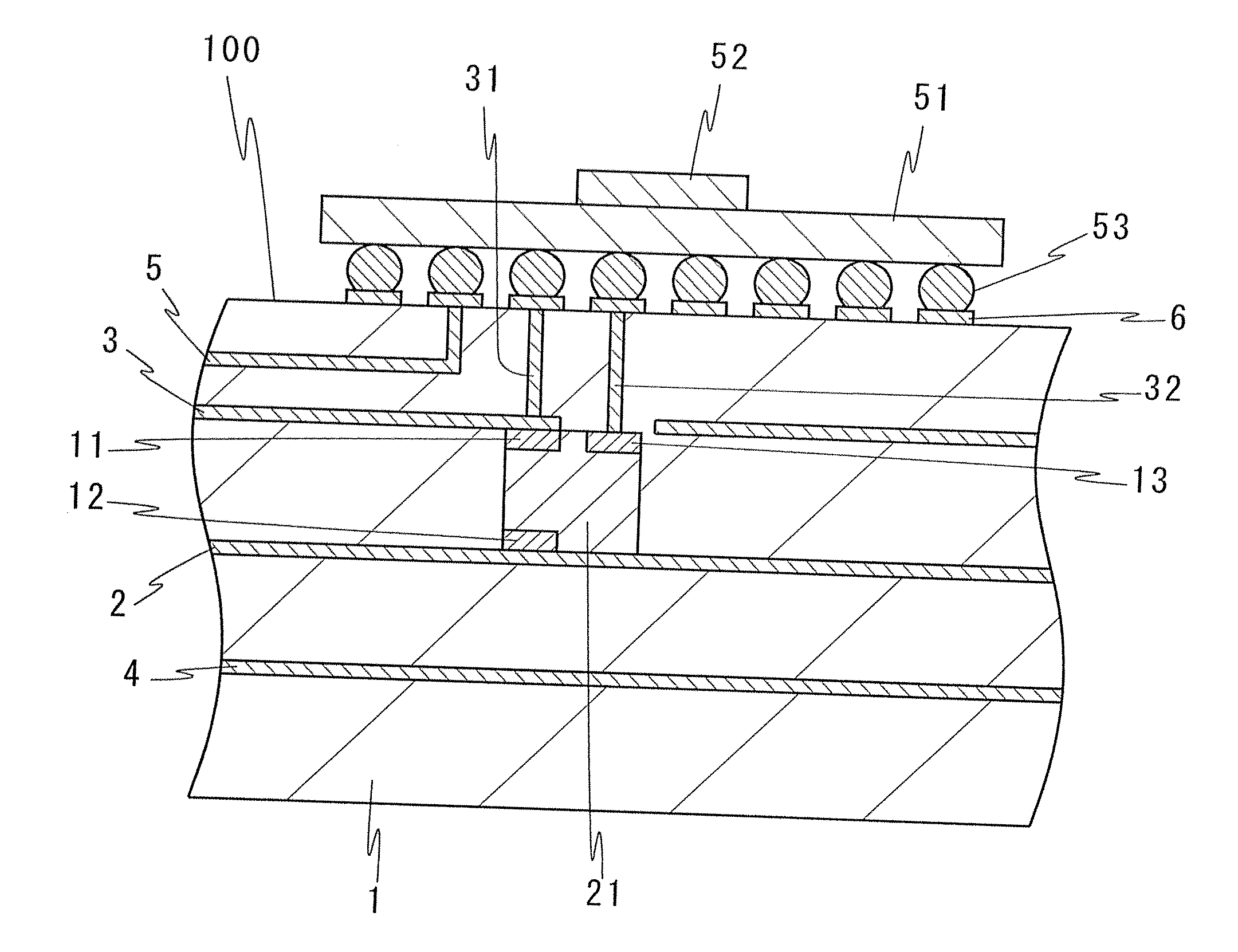
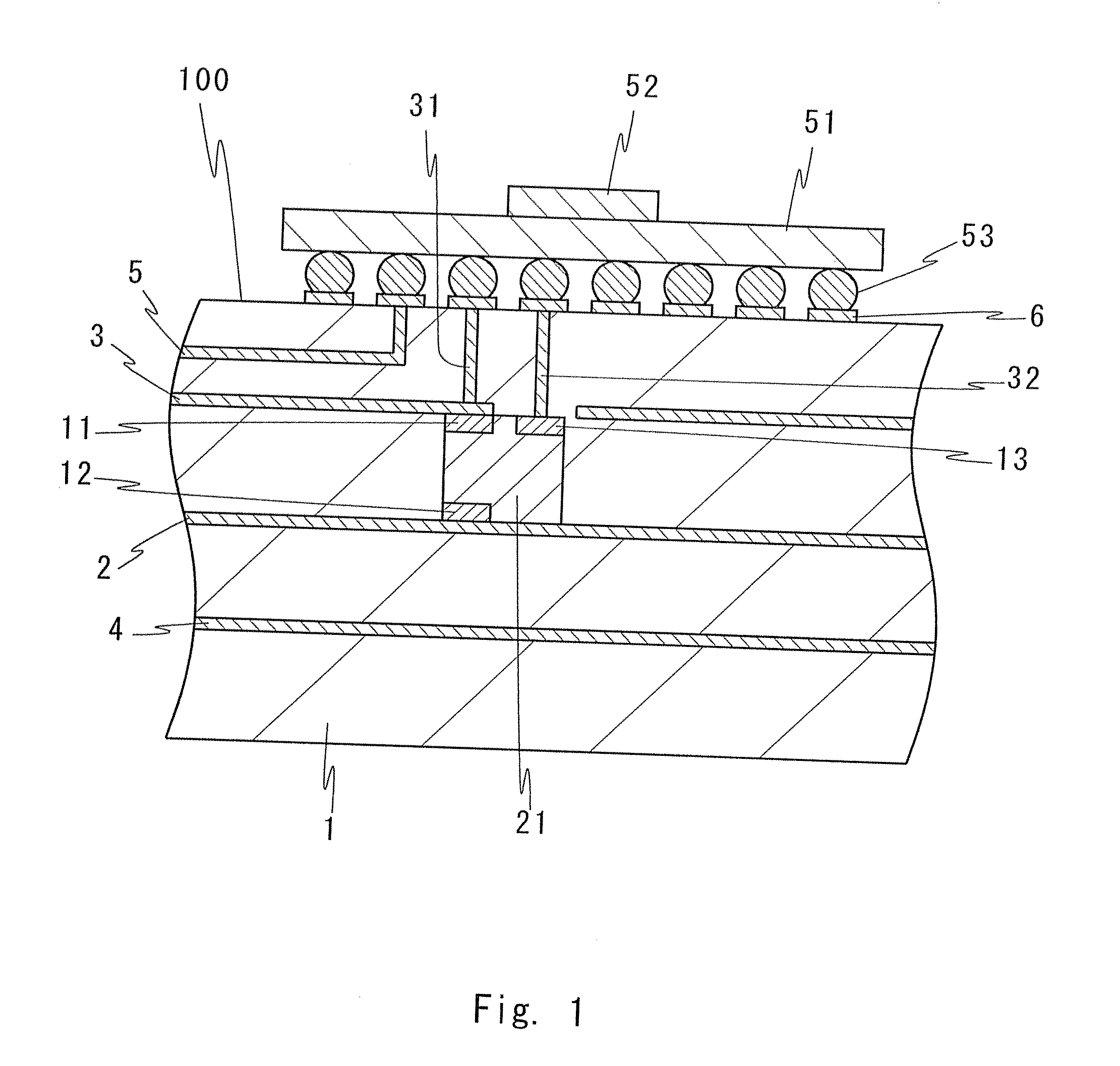
[0025]First, a printed circuit board (PCB) 100 according to a first exemplary embodiment of the present invention will be described. FIG. 1 is a sectional view showing a substantial part of the PCB 100 according to the first exemplary embodiment on which a semiconductor device is mounted. The PCB 100 is a printed circuit board, for example. As shown in FIG. 1, an LSI case 51 is mounted on the PCB 100. An LSI 52 is mounted on the LSI case 51. Pins 53 which connect the LSI case 51 with pads 6 are formed on a lower surface of the LSI case 51. The LSI case 51, the LSI 52, and the pins 53 constitute one semiconductor device. A plate-like member 1 extends in the horizontal direction of FIG. 1, but only a part of the plate-like member 1 is shown for simplicity of the drawing.

[0026]The PCB 100 includes the plate-like member 1, a high-voltage DC power supply plane 2, ground planes 3 and 4, a signal plane 5, the pads 6, a power supply circuit 21, and via holes 31 and 32. The high-voltage DC p...

second exemplary embodiment

[0035]Next, a printed circuit board (PCB) 200 according to a second exemplary embodiment of the present invention will be described. FIG. 3 is a sectional view showing a substantial part of the PCB 200 according to the second exemplary embodiment on which a semiconductor device will be described. As shown in FIG. 3, the PCB 200 has a configuration in which a signal line 10 is added to the PCB 100 according to the first exemplary embodiment. In the PCB 200, a power supply circuit 22 is provided in place of the power supply circuit 21 of the PCB 100. The other components of the PCB 200 are similar to those of the PCB 100, so the description thereof is omitted.

[0036]The power supply circuit 22 has a configuration in which a signal terminal 14 is added to the power supply circuit 21. The signal terminal 14 is supplied with a control signal from the outside of the PCB 200 through the signal line 10. The other components of the power supply circuit 22 are similar to those of the power sup...

third exemplary embodiment

[0039]Next, a printed circuit board (PCB) 300 according to a third exemplary embodiment of the present invention will be described. FIG. 4 is a sectional view showing a substantial part of the PCB 300 according to the third exemplary embodiment on which a semiconductor device is mounted. As shown in FIG. 4, the PCB 300 has a configuration in which a power supply circuit 23 is replaced with the power supply circuit 22 of the PCB 200 according to the second exemplary embodiment. The other components of the PCB 300 are similar to those of the PCB 200, so the description thereof is omitted.

[0040]The power supply circuit 23 includes a first power supply terminal 41, a second power supply terminal 42, a first high-voltage DC power supply terminal 43, a second high-voltage DC power supply terminal 44, the ground terminal 11, and the signal terminal 14. The first power supply terminal 41 and the second power supply terminal 42 are not connected to the ground plane 3 and independent from the...


PUM

PropertyMeasurementUnit
Poweraaaaaaaaaa
Electric potential / voltageaaaaaaaaaa
Areaaaaaaaaaaa

Abstract

A printed circuit board (PCB) according to an exemplary aspect of the present invention includes a plate-like member, a power supply circuit, a power supply line, and a ground line. The plate-like member has a surface on which a semiconductor device is mounted. The power supply circuit is embedded in the plate-like member in a region in which the semiconductor device is mounted, and outputs a power supply voltage and a ground voltage. The power supply line is formed in the plate-like member between the semiconductor device and the power supply circuit, and supplies the power supply voltage output from the power supply circuit to the semiconductor device. The ground line is formed in the plate-like member between the semiconductor device and the power supply circuit, and supplies the ground voltage output from the power supply circuit to the semiconductor device.

Description

INCORPORATION BY REFERENCE[0001]This application is based upon and claims the benefit of priority from Japanese patent application No. 2011-11882, filed on Jan. 24, 2011, the disclosure of which is incorporated herein in its entirety by reference.BACKGROUND OF THE INVENTION[0002]1. Technical Field[0003]The present invention relates to a printed circuit board (PCB) and a manufacturing method thereof, and more particularly, to a PCB that suppresses noise in power supplied to a mounted semiconductor device, and a manufacturing method thereof.[0004]2. Background Art[0005]There is a growing demand for a highly functional LSI in a system. In order to meet this demand, measures have been taken to increase clock speeds in each LSI. Since then, it has become difficult to further increase clock speeds due to limitations of semiconductor processes. For this reason, multi-core technology has been increasingly used as a method for improving the performance of each LSI. In the multi-core technolo...

Claims


Application Information

Patent Timeline
IPC IPC(8): H05K1/00H05K3/10
CPCH05K1/0243H05K1/0262Y10T29/49155H05K1/185H05K2201/0792H05K1/113H01L2224/04105H01L2224/12105H01L2224/2518H01L2224/20H01L2924/15311
Inventor NAKANO, TOSHIHIKO
Owner NEC CORP
Learn More