Semiconductor element and solid-state imaging device

a solid-state imaging and semiconductor technology, applied in the direction of radio frequency controlled devices, instruments, television systems, etc., can solve the problems of complex structure of conventional image sensors that use lock-in pixels, and also generate transfer delay problems, etc., to achieve good transfer efficiency of charges, simple structure of pixels, and high resolution

Active Publication Date: 2012-08-02
NAT UNIV CORP SHIZUOKA UNIV
View PDF38 Cites 26 Cited by
  • Summary
  • Abstract
  • Description
  • Claims
  • Application Information

AI Technical Summary

Benefits of technology

[0015]According to the present invention, it is possible to provide a solid-state imaging device in which the trouble that the potential gradient becomes zero at the vicinity of the center on the transferring-path of charges is removed, and the potential gradient is generated in the overall width of the ch...

Problems solved by technology

Consequently, the conventional image sensor that uses the lock-in pixels is intricate in structure.
Also, in the case of the transfer through the gate structure of...

Method used


Image

  • Semiconductor element and solid-state imaging device
  • Semiconductor element and solid-state imaging device
  • Semiconductor element and solid-state imaging device

Examples


first embodiment

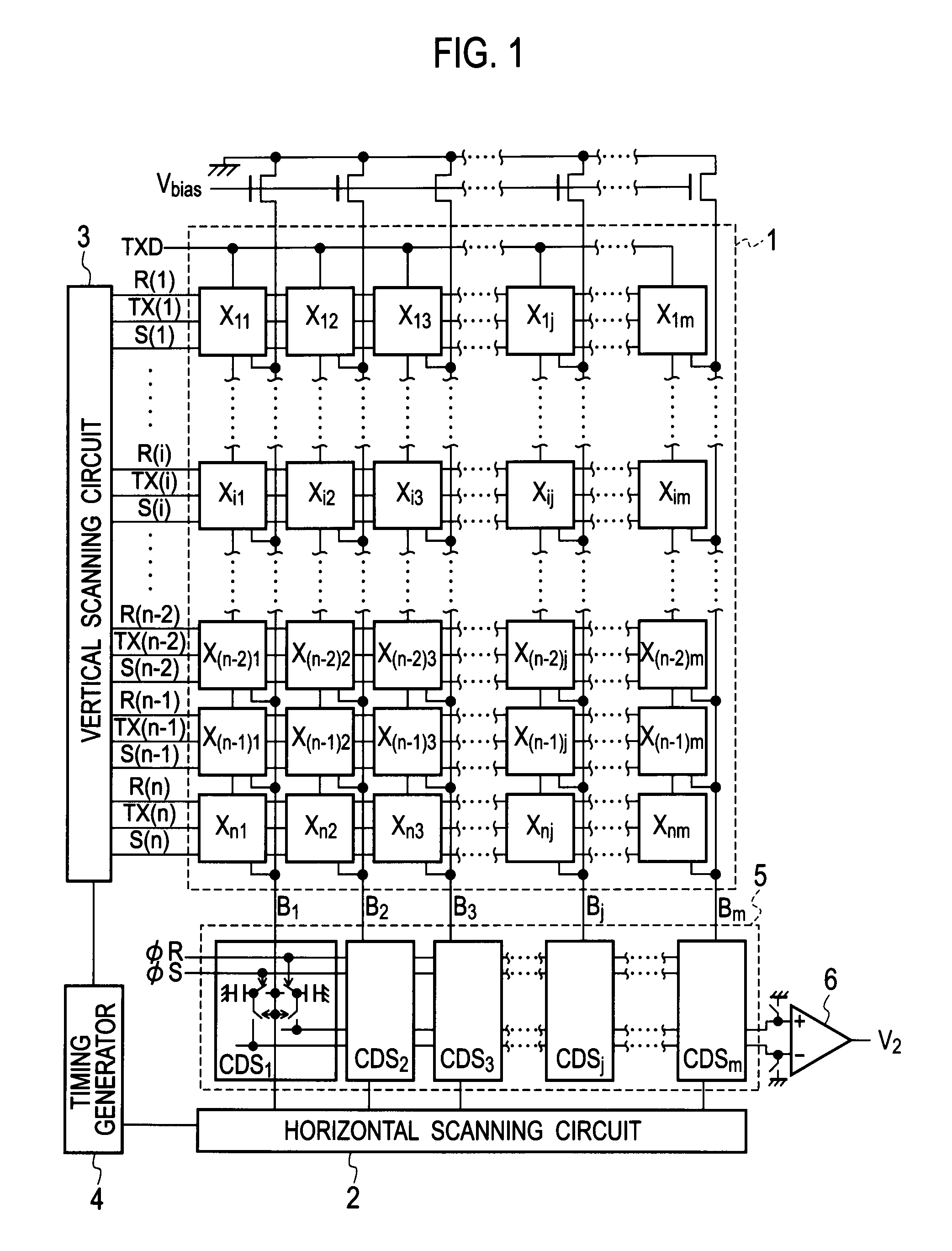
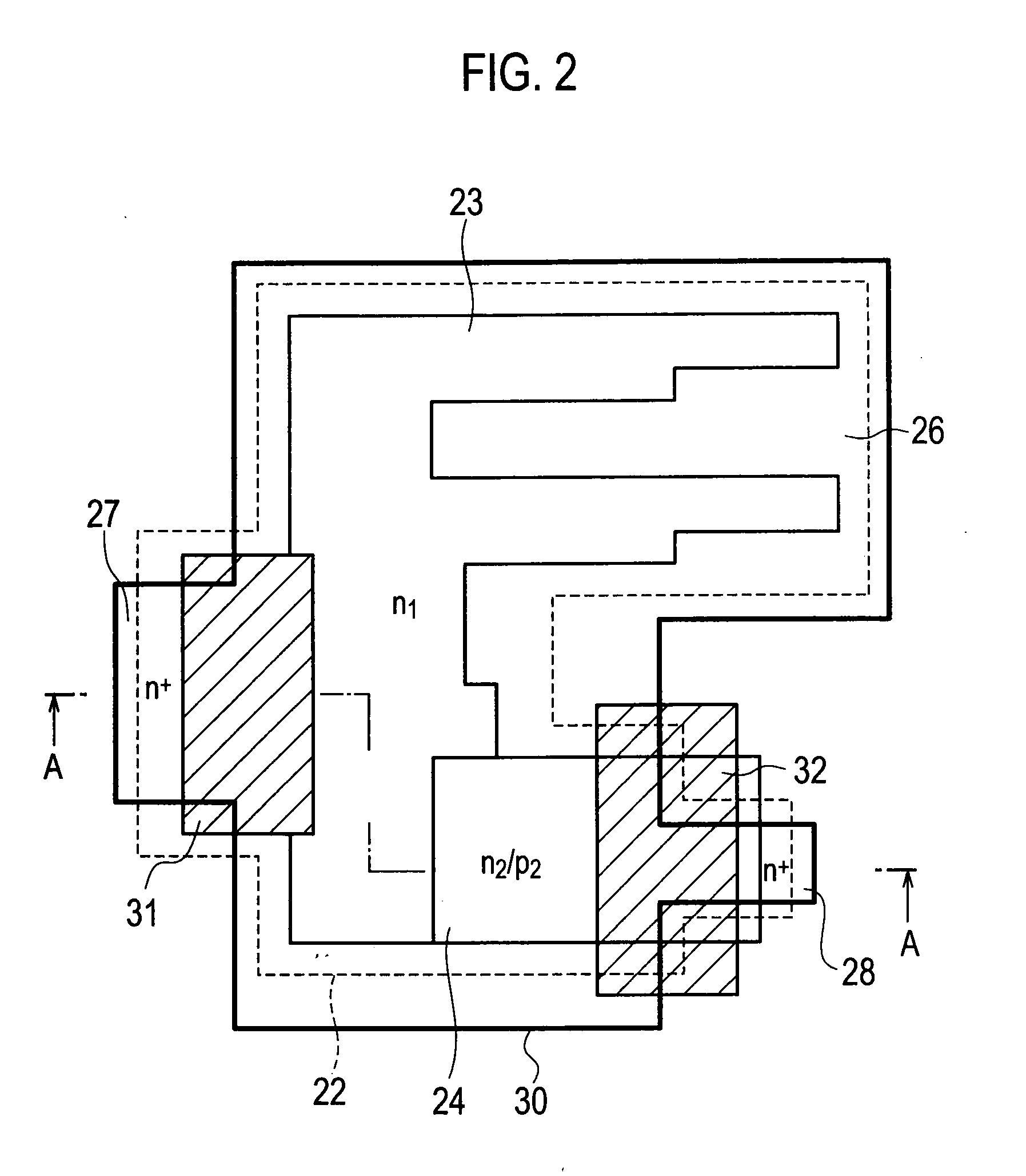
[0033]In a solid-state imaging device (two-dimensional image sensor) pertaining to a first embodiment of the present invention, as illustrated in FIG. 1, a pixel array 1 and peripheral circuits (2, 3, 4, 5 and 6) are integrated on a same semiconductor chip. In the pixel array 1, a large number of pixels Xij (i=1 to m; j=1 to n: where m, n are integers, respectively) are arrayed in a shape of a two-dimensional matrix, and for example, a rectangular imaging region is established. On the lower side of the pixel array 1, a horizontal scanning circuit 2 is provided along pixel rows X11 to X1m; - - - ; Xi1 to Xim; - - - ; X(n-2)1 to X(n-2)m; X(n-1)1 to X(n-1)m; and Xn1 to Xnm directions. On the left side of the pixel array, a vertical scanning circuit 3 is provided along pixel columns X11, - - - , Xi1, - - - , X(n-2)1, X(n-1)1, Xn1; X12, - - - , Xi2, - - - ; X(n-2)2, X(n-1)2, Xn2; X13, - - - , Xi3, - - - ; X(n-2)3, X(n-1)3, Xn3; - - - ; X1j, - - - , Xij, - - - , X(n-2)j, X(n-1)j, Xnj; - -...

second embodiment

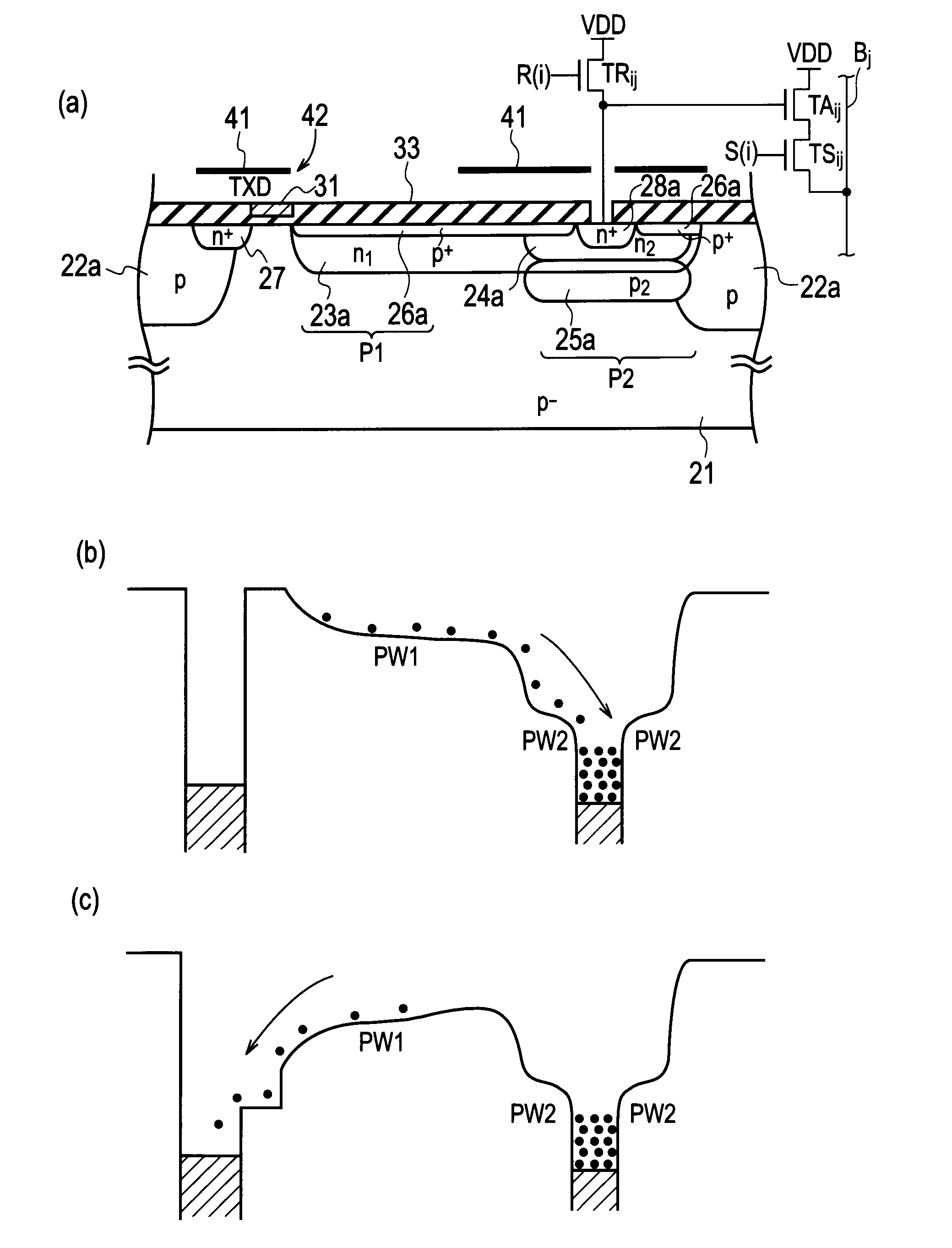
[0077]In the pixel in the solid-state imaging device pertaining to the first embodiment, by controlling the potential of the read-out gate electrode 32, charges accumulated in the accumulation region 24 are transferred to the read-out region 28. However, as illustrated in a plan view in FIG. 8, by designing a semiconductor element serving as a part of the pixel Xij in the solid-state imaging device such that the read-out region 28a is allocated in the inside of a buried region 23a, and furthermore in the inside of an accumulation region 24a, without providing the read-out gate electrode, charges accumulated in the accumulation region 24a can be directly transferred to the read-out region 28.

[0078]As FIG. 9 (a) illustrates a step-formed cross-sectional view taken from B-B direction in FIG. 8, the pixel (semiconductor element) in a solid-state imaging device pertaining to a second embodiment of the present invention encompasses a semiconductor region 21 of the first conductivity type ...

third embodiment

[0087]Also, as illustrated in FIGS. 8 and 9, the already-described second embodiment has represented a structure such that the read-out region 28a is located at the vicinity of the center in the surface of the accumulation region 24a, the block layer 25a of the first conductivity type (p+-type), which is higher in impurity concentration than the semiconductor region 21, is provided below the accumulation region 24a, and without any read-out gate electrode, charges accumulated in the accumulation region 24 are directly transferred to the read-out region 28. However, in a semiconductor element serving as a part of the pixel Xij in a solid-state imaging device pertaining to a third embodiment of the present invention, as illustrated in FIG. 11, a layout is employed such that the areas of the accumulation region 24a and the block layer 25a which have been used in the second embodiment are removed, and a well region (p-well) 22b overlaps with a read-out region 28b. In the plan view in FI...


PUM


Abstract

A solid-state imaging device includes a semiconductor region of p-type; a buried region of n-type, configured to serve as a photodiode together with the semiconductor region; a extraction region of n-type, configured to extract charges generated by the photodiode from the buried region, having higher impurity concentration than the buried region; a read-out region of n-type, configured to accumulate charges, which are transferred from the buried region having higher impurity concentration than the buried region; and a potential gradient changing mechanism, configured to control a potential of the channel, and to change a potential gradient of a potential profile from the buried region to the read-out region and a potential gradient of a potential profile from the buried region to the extraction region, so as to control the transferring/extraction of charges.

Description

TECHNICAL FIELD[0001]The present invention relates to a semiconductor element that has a function for modulating detected electrons, which are generated by light, in a time domain, and a solid-state imaging device in which these semiconductor elements are arrayed one-dimensionally or two-dimensionally.BACKGROUND ART[0002]A sensor element disclosed in “DEVICE AND METHOD FOR THE DETECTION AND DEMODULATION OF AN INTENSITY-MODULATED RADIATION FIELD (see patent literature (PTL) 1)” published in 1994, or in other documents, which has a function for modulating, in a time domain, the detection of electrons generated by light in a pixel, is referred to as a “lock-in pixel”. By applying the sensor element encompassing the lock-in pixels to a buried photodiode structure used in recent CMOS image sensors, if a lock-in image sensor can be established, because the sensor element is superior in mass productivity, a realization of a high performance image sensor being manufactured at low price is e...

Claims


Application Information

Patent Timeline
IPC IPC(8): H01L27/148H01L31/102G01S7/4863G01S17/894
CPCG01S7/4816G01S7/4863H01L27/14609H01L27/14656H01L27/14612H04N5/37452H04N5/378H01L27/14603H01L27/14607H04N5/359G01S17/894H04N25/62H04N25/771H04N25/75H01L27/146H04N25/00
Inventor KAWAHITO, SHOJISAWADA, TOMONARI
Owner NAT UNIV CORP SHIZUOKA UNIV
Why Eureka
Try Eureka