Package stack device and fabrication method thereof

a technology of packaging stack and fabrication method, which is applied in the direction of semiconductor devices, semiconductor/solid-state device details, electrical devices, etc., can solve the problems of positional deviation of joints between the two package structures, adversely affecting product yield, and difficult control, so as to facilitate vertical stacking of the package structure, avoid surface contamination, and easy control

Active Publication Date: 2012-08-02
UNIMICRON TECH CORP
View PDF2 Cites 47 Cited by
  • Summary
  • Abstract
  • Description
  • Claims
  • Application Information

AI Technical Summary

Benefits of technology

[0018]Therefore, the present invention stacks and electrically connects two package structures through a plurality of metal posts so as to avoid contamination of surfaces of the package structures by a solder material as in the prior art. Further, variation in the size of the metal posts is easy to control, thereby facilitating vertical stacking of the package structures and overcoming the conventional problem of joint deviation.
[0019]Furthermore, variation in the heights of the metal posts does not change the diameters of the metal posts and accordingly the surface area occupied by the metal posts does not increase, thereby avoiding reduction of available spaces for circuits and electronic elements.
[0020]Furthermore, by forming the metal posts through electroplating, the present invention avoids the risk of bridging when the metal posts are increased in height, thus increasing the product yield.
[0021]Moreover, warpage of the substrates are prevented since the package structures are supported by the metal posts and the gap between the first and second package structures is filled with the encapsulant.

Problems solved by technology

Further, variation in the size of the solder balls 110 is not easy to control, which can easily adversely affect vertical stacking of the two package structures and even cause positional deviation of joints between the two package structures.
Moreover, increased size of the solder balls 110 can easily cause bridging between the solder balls, thus adversely affecting the product yield.

Method used


Image

  • Package stack device and fabrication method thereof
  • Package stack device and fabrication method thereof
  • Package stack device and fabrication method thereof

Examples


Embodiment Construction

[0024]The following illustrative embodiments are provided to illustrate the disclosure of the present invention, these and other advantages and effects can be apparent to those in the art after reading this specification.

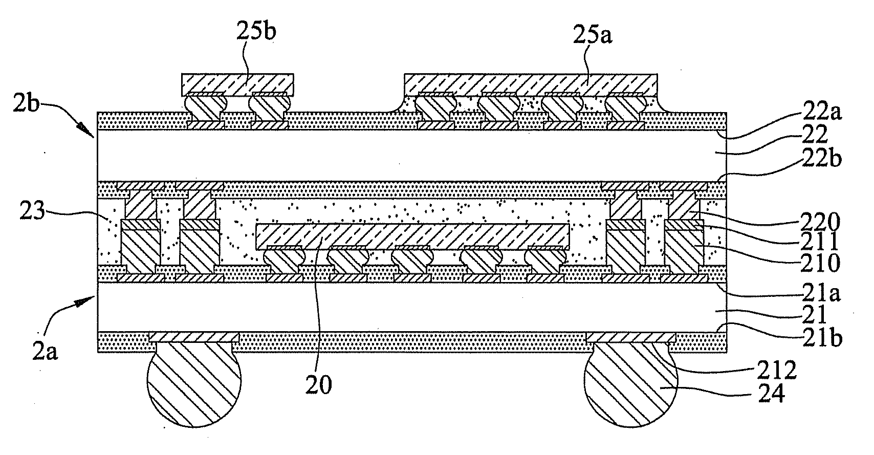
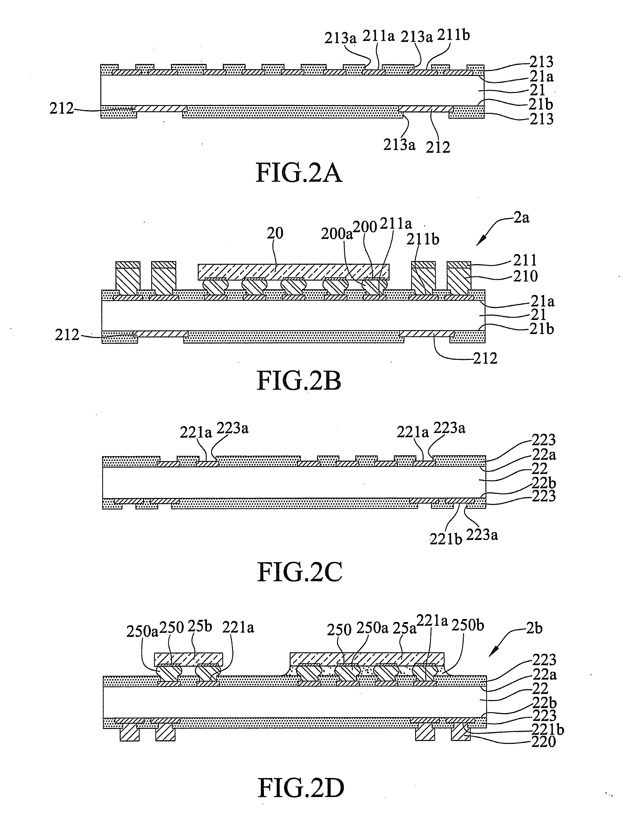
[0025]FIGS. 2A to 2G are cross-sectional views showing a fabrication method of a package stack device according to the present invention. Referring to FIG. 2A, a first substrate 21 having a first surface 21a and a second surface 21b opposite to the first surface 21a is provided. The first surface 21a of the first substrate 21 has a plurality of solder pads 211a and a plurality of conductive pads 211b. The second surface 21b of the first substrate 21 has a plurality of ball pads 212.

[0026]In the present embodiment, an insulating protection layer 213 such as a solder mask layer is formed on the first and second surfaces 21a, 21b of the first substrate 21, and a plurality of openings 213a are formed in the insulating protection layer 213 for exposing the solder pads 21...


PUM


Abstract

A package stack device includes a first package structure having a plurality of first metal posts and a first electronic element disposed on a surface thereof, a second package structure having a plurality of second metal posts and a second electronic element disposed on opposite surfaces thereof, and an encapsulant formed between the first and second package structures for encapsulating the first electronic element. By connecting the first and second metal posts, the second package structure is stacked on the first package structure with the support of the metal posts and the encapsulant filling the gap therebetween so as to prevent warpage of the substrate.

Description

BACKGROUND OF THE INVENTION[0001]1. Field of the Invention[0002]The present invention relates to package stack devices and fabrication methods thereof, and more particularly, to a package stack device having a plurality of package structures stacked on each other and a fabrication method thereof.[0003]2. Description of Related Art[0004]Along with the development of semiconductor packaging technology, various types of packages haven been developed for semiconductor devices. In order to further enhance electrical performance and reduce package size, a plurality of package structures are stacked on each other to form a POP (package on package) device. As such, electronic elements having difference functions, such as memories, CPUs(central processing units), GPUs (graphics processing units), image application processors and the like, can be integrated together so as to be applied in various kinds of thin-type electronic products. FIG. 1 schematically illustrates a cross-sectional view o...

Claims


Application Information

Patent Timeline
Patent Type & Authority Applications(United States)
IPC IPC(8): H01L23/488H01L21/56
CPCH01L21/56H01L23/3128H01L25/105H01L25/162H01L2225/1023H01L2924/3511H01L2224/16225H01L2224/32225H01L2224/73204H01L23/49816H01L2225/1058H01L2924/00H01L2924/00012H01L23/49811
Inventor HU, CHU-CHINHSU, SHIH-PINGCHEN, YI-JU
Owner UNIMICRON TECH CORP
Why Eureka
Try Eureka