Flip-chip packaging for dense hybrid integration of electrical and photonic integrated circuits

a technology of integrated circuits and flip-chips, applied in the field of chip packaging, can solve the problems of high channel data rate, limited packaging approach, and limited packaging approach of commercial optical transceivers, transmitters (tx) and receivers that utilize integrated photonic chips (e.g., si photonics or inp)

Inactive Publication Date: 2012-08-16
IBM CORP
View PDF15 Cites 61 Cited by
  • Summary
  • Abstract
  • Description
  • Claims
  • Application Information

AI Technical Summary

Benefits of technology

[0009]A method for fabricating an optical signaling device includes flip-chip bonding a photonics chip and an electrical integrated circuit (IC) using a first solder to form an optochip; flip-chi

Problems solved by technology

Commercial optical transceiver (TRX), transmitter (TX) and receiver (RX) implementations that utilize integrated photonics chips (e.g., Si photonics or InP) are limited to low-density w

Method used


Image

  • Flip-chip packaging for dense hybrid integration of electrical and photonic integrated circuits
  • Flip-chip packaging for dense hybrid integration of electrical and photonic integrated circuits
  • Flip-chip packaging for dense hybrid integration of electrical and photonic integrated circuits

Examples


Embodiment Construction

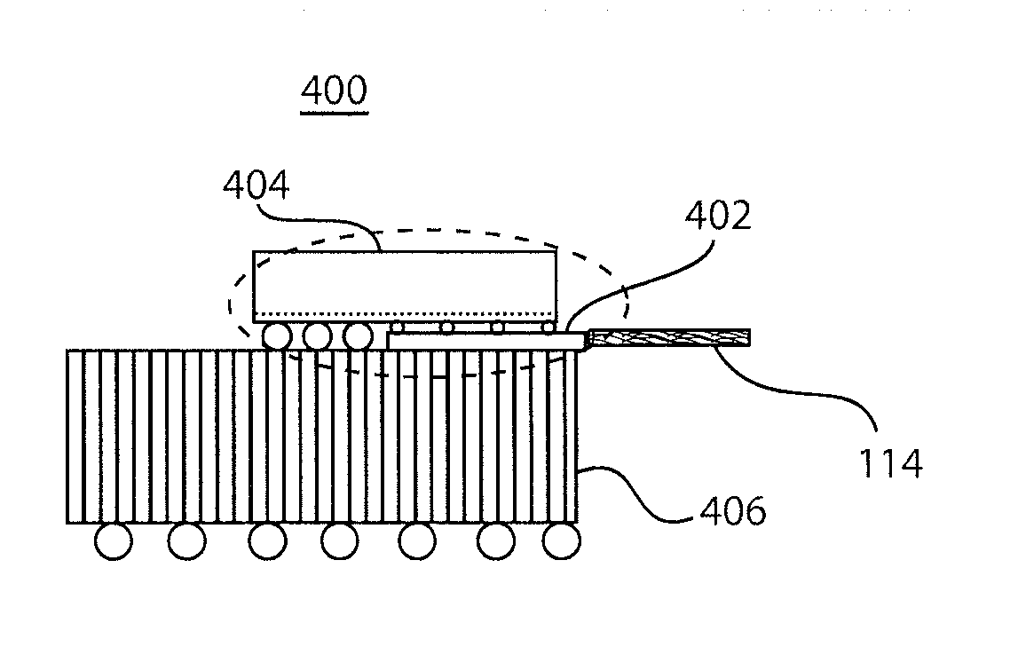
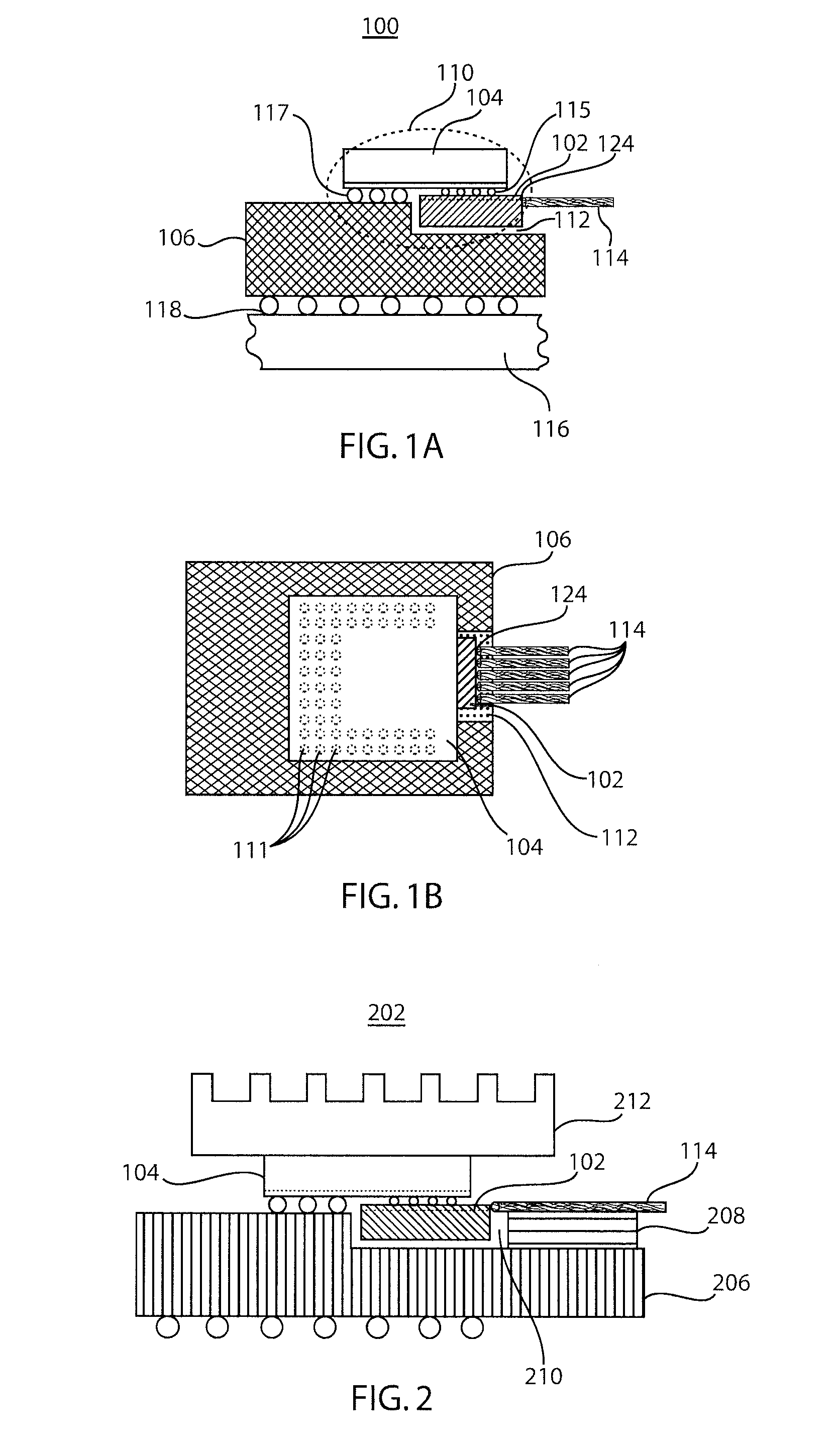
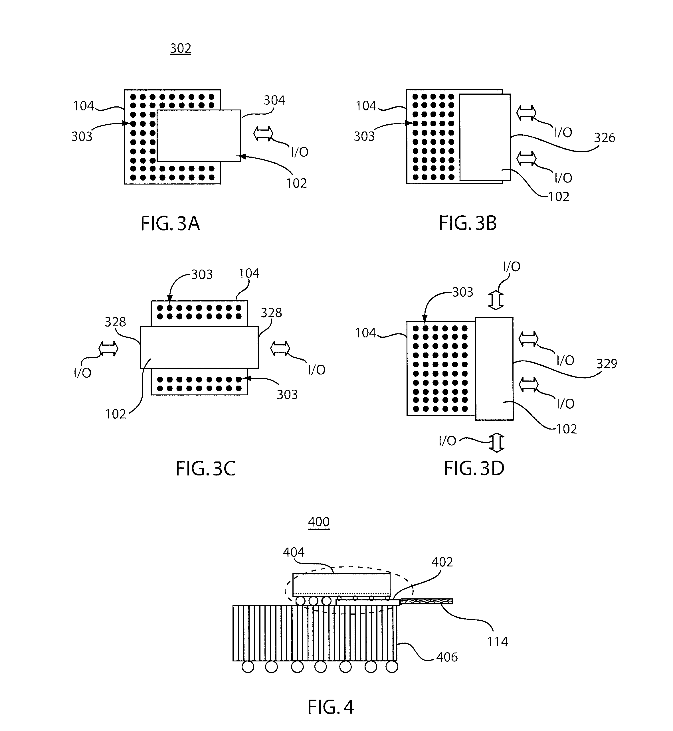
[0023]In accordance with the present principles, highly-integrated hybrid packaging is employed that exclusively utilizes flip-chip bonding to construct dense, low-power and high-speed transmitter (TX), receiver (RX), and / or transceiver (TRX) modules. In useful embodiments, hybrid integration of two components includes a photonic optical chip and an electrical integrated circuit (IC). A resulting component is an optochip, which is a component with high-speed optical functionality that is further flip-chip packaged to an organic or ceramic carrier. One preferred substrate material for the photonic chip is Si.

[0024]Photonic circuits offer extremely high-density integration (nm-scale), complementary metal oxide semiconductor (CMOS) and SiGe bipolar process compatibility, and low fabrication cost. Optical devices (e.g., modulators and detectors) have been demonstrated to operate at speeds up to 40 Gb / s and beyond. In addition, wavelength division multiplexing (WDM) can be straightforwar...


PUM


Abstract

A chip system and method includes a photonics chip and an electrical integrated circuit (IC) flip-chip coupled to the photonics chip to form an optochip. The IC or the photonics chip includes an array of bond pads for attachment to the other. The optochip has an array of bond pads for subsequent attachment to a carrier where the photonics chip includes an exposed edge to connect with at least one waveguide.

Description

GOVERNMENT RIGHTS[0001]This invention was made with Government support under Contract No. HR0011-08-C-0102 awarded by the Defense Advanced Research Projects Agency (DARPA). The Government has certain rights in this invention.BACKGROUND[0002]1. Technical Field[0003]The present invention relates to chip packaging and more particularly to hybrid integration configurations for electrical and photonic chips.[0004]2. Description of the Related Art[0005]Flip-chip technology includes methods for interconnecting semiconductor devices, such as integrated circuit (IC) chips to external circuitry using solder bumps that have been deposited onto chip pads. The solder bumps are deposited on the chip pads on a top side of a wafer to mount the chip to external circuitry (e.g., a circuit board or another chip or wafer). The wafer is flipped over so that its top side faces down, and aligned so that its pads align with matching pads on the external circuit, and then the solder is flowed to complete th...

Claims


Application Information

Patent Timeline
IPC IPC(8): G02B6/12H01L33/48
CPCH01L27/144G02B6/426
Inventor DOANY, FUAD E.LEE, BENJAMIN G.SCHOW, CLINT L.
Owner IBM CORP
Why Eureka
Try Eureka