Serdes power throttling as a function of detected error rate

Active Publication Date: 2012-08-23
QUALCOMM INC
View PDF20 Cites 41 Cited by
  • Summary
  • Abstract
  • Description
  • Claims
  • Application Information

AI Technical Summary

Benefits of technology

[0013]Error detection and correction circuitry is provided in the SerDes receivers of both the first and second SerDes links. This error detection and correction circuitry can detect one or more bit errors in a SerDes communication and correct a single bit error. By providing this error detection and correction circuitry, the need to retransmit to successfully communicate data across a SerDes link is reduced despite the fact that the lower bounds of the acceptable bit error rate ranges are set to be substa

Problems solved by technology

These SerDes links have tended to be relatively expensive and generally have consumed large amounts of power.
SerDes links have therefore generally not been considered suitable for use in mobile devices (such as cellular telephones) where keeping power consumption low is very important.
As a result, this first example of power saving is only minimally effective in reducing power consumption.
This circuitry may consume a lot of power.
Unfortunately, there is an amount of time required to turn these circuits back on (settling and lock time of the PLL) and have them functional again.
If these circuits are in their off states when t

Method used


Image

  • Serdes power throttling as a function of detected error rate
  • Serdes power throttling as a function of detected error rate
  • Serdes power throttling as a function of detected error rate

Examples


Embodiment Construction

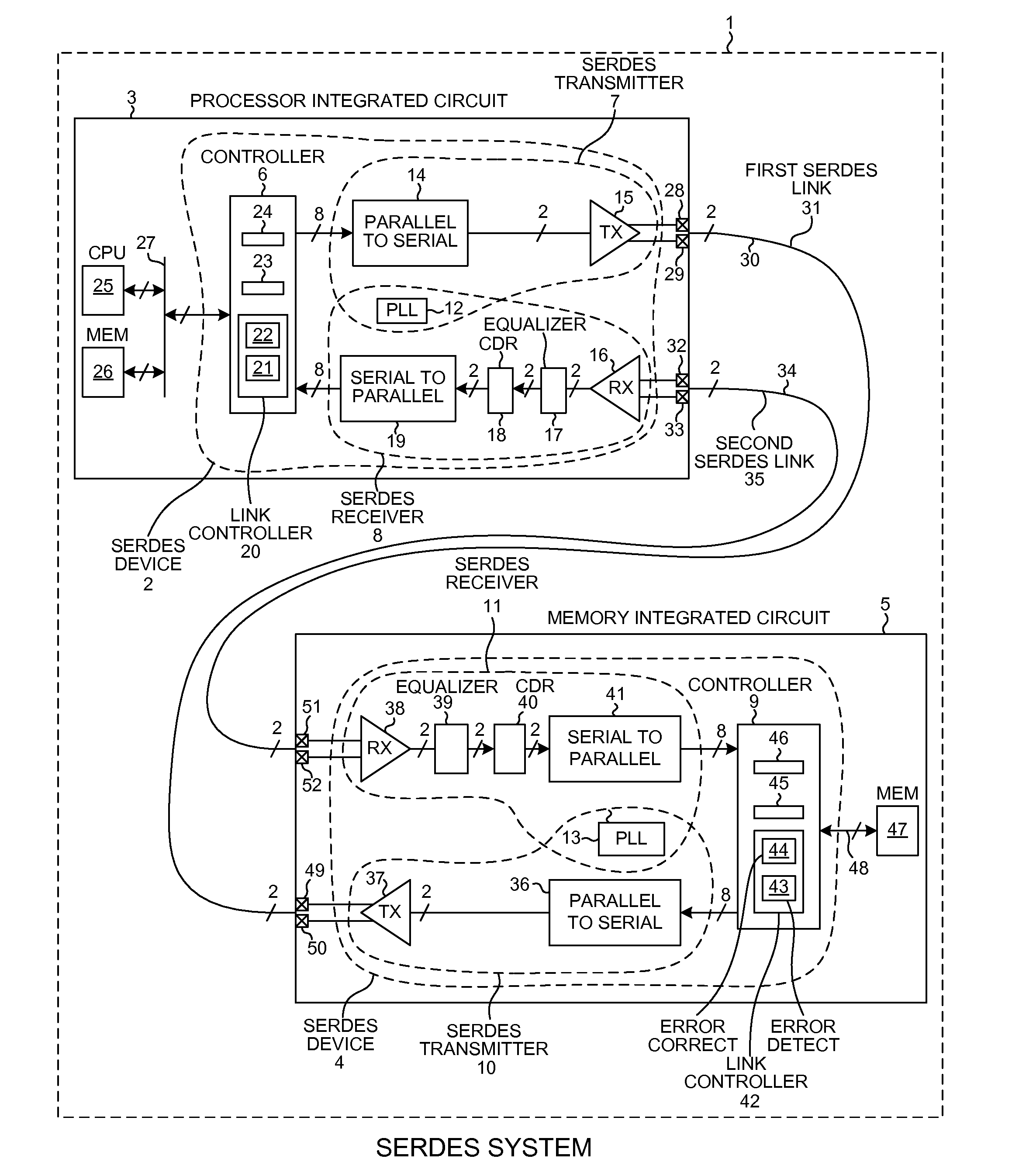
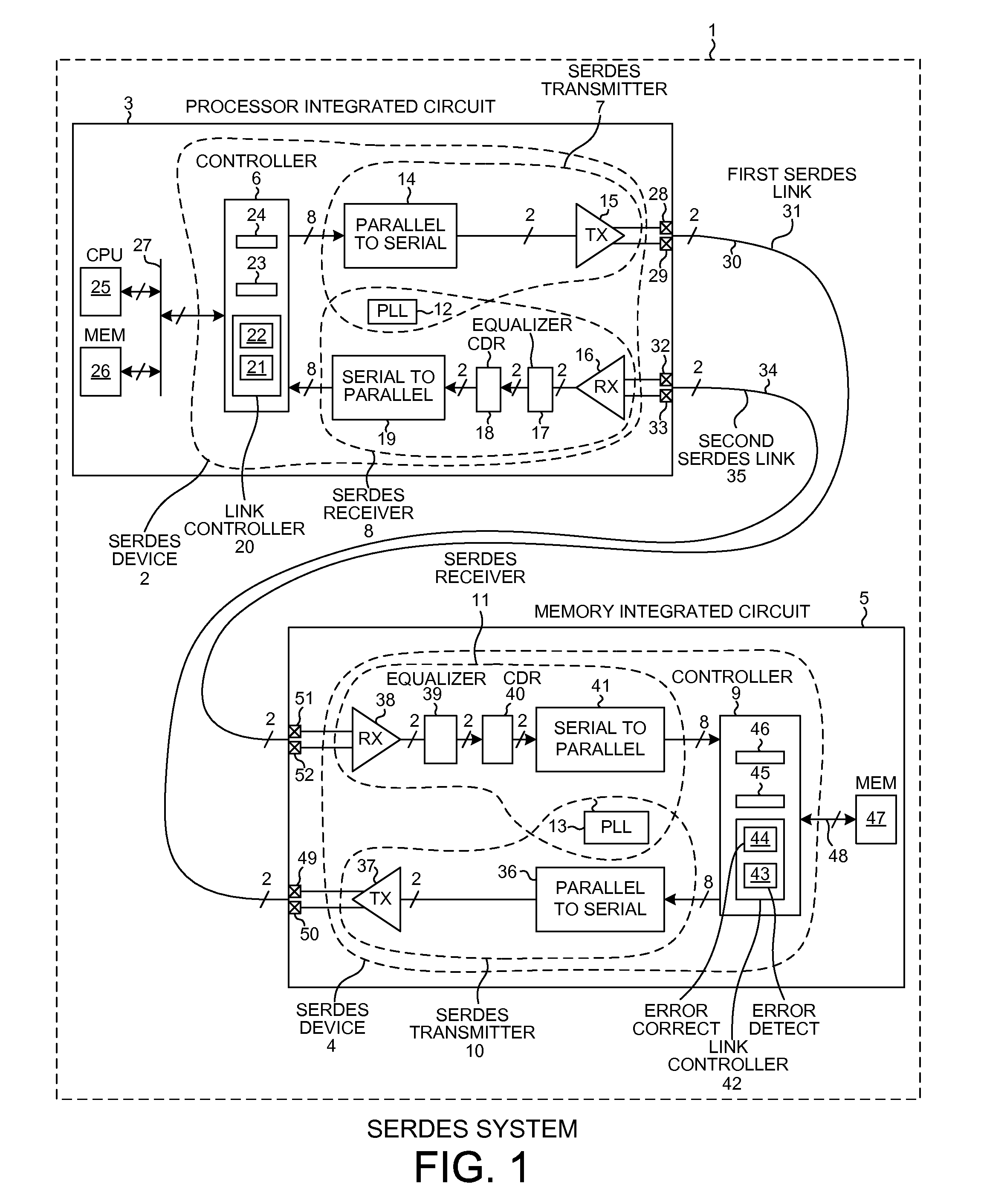
[0039]FIG. 1 is a diagram of a system 1 involving involves a SerDes device 2 in a processor integrated circuit 3 and a SerDes device 4 in a memory integrated circuit 5. In one example, system 1 is a battery-powered wireless mobile communication device such as a cellular telephone handset. SerDes device 2 includes a controller portion 6, a SerDes transmitter portion 7 and a SerDes receiver portion 8. SerDes device 4 includes a controller portion 9, a SerDes transmitter portion 10 and a SerDes receiver portion 11. A Phase-Locked Loop (PLL) 12 in the SerDes device 2 of the processor integrated circuit 3 is considered to be both part of the SerDes transmitter portion 7 and part of the SerDes receiver portion 8. Likewise, a PLL 13 in the SerDes device 4 of the memory integrated circuit 5 is considered to be both part of the SerDes transmitter portion 10 and part of the SerDes receiver portion 11.

[0040]The SerDes transmitter portion 7 of the processor integrated circuit 3 includes a paral...


PUM


Abstract

A system involves a first SerDes link from a first integrated circuit (IC) to a second IC and a second link from the second IC to the first IC. Power consumption settings in circuitry of the first link are adjusted to control power consumption such that the bit error rate of the first link is maintained in a range, where the lower bound of the range is substantially greater than zero. Power consumption settings in circuitry for the second link are adjusted to control power consumption such that the bit error rate of the second link is maintained in range, where the lower bound of the range is substantially greater than zero. In one example, circuitry in the second IC detects errors in the first link and reports back via the second link. The first IC uses the reported information to determine a bit error rate for the first link.

Description

BACKGROUND INFORMATION[0001]1. Technical Field[0002]The present disclosure relates to Serial / Deserializer (SerDes) devices.[0003]2. Background Information[0004]Traditionally, the bus in a computer between the computer's Central Processing Unit (CPU) and the computer's main memory was a parallel bus. As the processing throughput of computers increased, and as demands on memory bandwidth increased, it became increasingly common for the bus between the CPU and memory to be implemented as one or more Serializer / Deserializer (SerDes) links. These SerDes links have tended to be relatively expensive and generally have consumed large amounts of power. SerDes links have therefore generally not been considered suitable for use in mobile devices (such as cellular telephones) where keeping power consumption low is very important. Recently, however, there has been a movement to use SerDes or SerDes-like technologies in low power mobile devices such as cellular telephones. For example, there is a...

Claims


Application Information

Patent Timeline
IPC IPC(8): G06F11/00
CPCH04L25/02H04L12/12H04W52/0209H04L1/0001H04L1/0036Y02D30/70G06F11/00G06F13/00
Inventor CHUN, DEXTER T.WOLF, JACK K.SUH, JUNGWONSOWLATI, TIRDAD
Owner QUALCOMM INC
Why Eureka
Try Eureka