Attachment for substrates having different diameters, substrate processing apparatus, and method of manufacturing substrate or semiconductor device

Inactive Publication Date: 2012-08-30
KOKUSA ELECTRIC CO LTD
View PDF6 Cites 298 Cited by
  • Summary
  • Abstract
  • Description
  • Claims
  • Application Information

AI Technical Summary

Benefits of technology

[0009]Meanwhile, in order to reduce costs of a substrate processing apparatus, regardless of a diameter of a wafer to be processed, components forming the substrate processing apparatus, for example, a transfer system for transferring the wafer, may be standardized as much as possible. In addition, as disclosed in Patent Document 1, in the substrate processing apparatus in which two kinds of reactive gases ar

Problems solved by technology

However, since a size of a wafer which is actually processed is generally 2 to 4 inches, the 2- to 4-inch wafers cannot be simply processed under environments corresponding to the 8-inch wafer.
Meanwhile, like the substrate processing apparatus disclosed in Patent Document

Method used


Image

  • Attachment for substrates having different diameters, substrate processing apparatus, and method of manufacturing substrate or semiconductor device
  • Attachment for substrates having different diameters, substrate processing apparatus, and method of manufacturing substrate or semiconductor device
  • Attachment for substrates having different diameters, substrate processing apparatus, and method of manufacturing substrate or semiconductor device

Examples


first embodiment

Typical Effects of First Embodiment

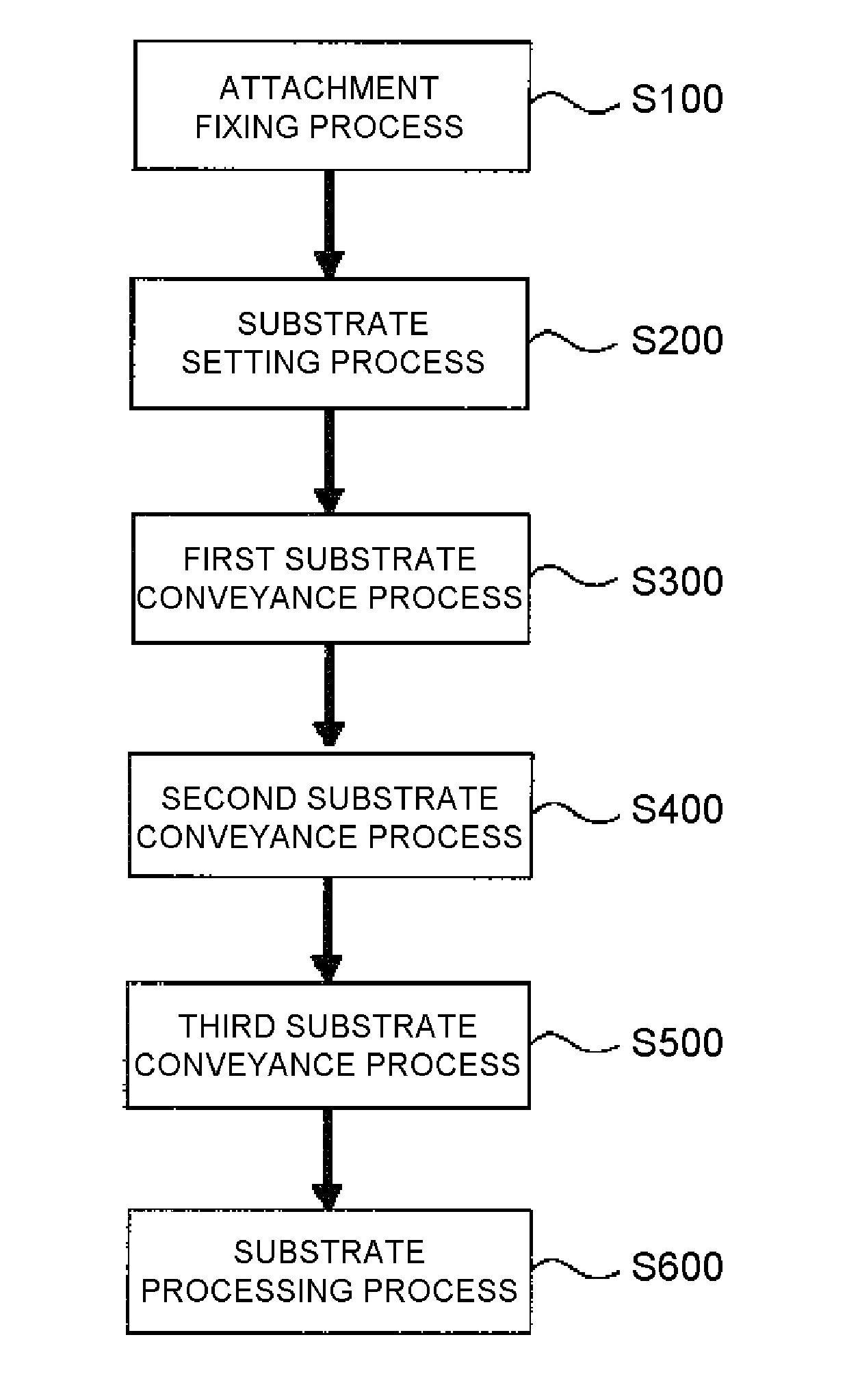
[0141]According to the technical spirit described with reference to the first embodiment, at least one of a plurality of effects described below will be provided.

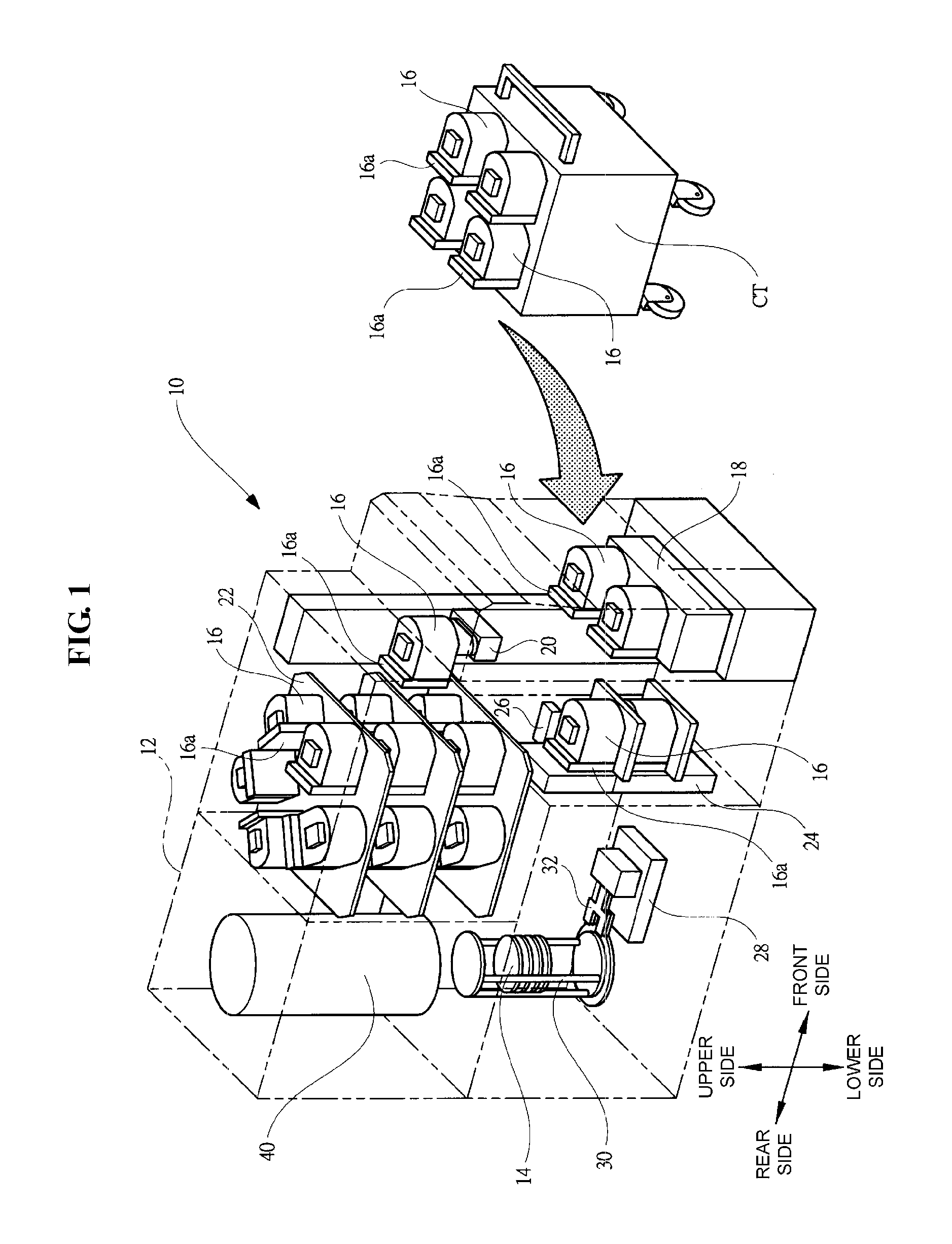
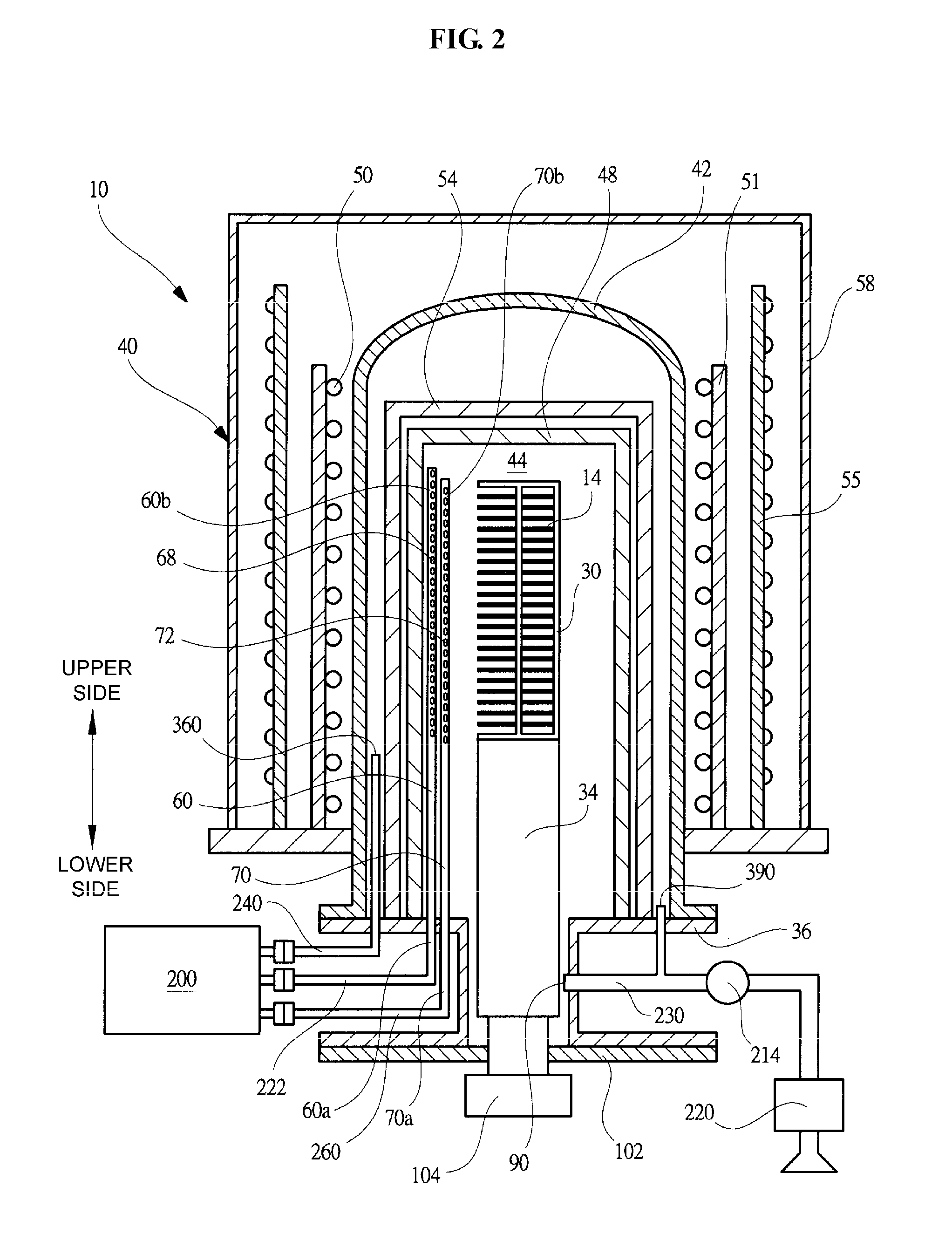
[0142](1) According to the first embodiment, the upper plate 401 and the lower plate 402 supported by the first support grooves 16e that can support the 8-inch (first size) wafer, and the holding columns 403a to 403c each including the second support grooves 404 installed at the upper plate 401 and the lower plate 402 and capable of supporting the wafer 14, which is the 2-inch (second size) wafer smaller than the first size (if necessary, via the wafer holder 100 and the holder member 405) are provided. Accordingly, the downsized wafers 14 having the second size can be housed in the pod 16 corresponding to the wafers having the first size, and the pod 16, which is a transfer system, may be standardized to reduce costs of the semiconductor manufacturing apparatus 10. In addition, since a la...

second embodiment

Typical Effects of Second Embodiment

[0158]The technical spirit described in the second embodiment may have substantially the same effects as the first embodiment. In addition, in the second embodiment, since contact portions of the front ends 503 of the spring members 501 may be disposed at the same positions as outer diameter portions of the upper plate 401 and the lower plate 402, the pod and the cover for an 8-inch (a first size) wafer can be used as they are, and standardization may be further advanced. Further, since a structure of the pressing member can be simplified in comparison with the first embodiment, the semiconductor manufacturing apparatus 10 can be reduced in cost.

Third Embodiment

[0159]Hereinafter, a third embodiment of the present invention will be described in detail with reference to the accompanying drawings. In addition, components having the same functions as the other embodiments will be designated by the same reference numerals, and detailed description ther...

third embodiment

Typical Effects of Third Embodiment

[0167]The technical spirit described in the third embodiment may have substantially the same effects as the other embodiments. In addition, in the third embodiment, in comparison with the above-mentioned embodiments, the holding columns, which are holding members, may be omitted. Further, since the plate-shaped members 601 are supported by the first support grooves 16e of the pod 16, respectively, the number of wafers 14 housed in the pod 16 can be increased and efficiency in a film-forming process can be increased.

Fourth Embodiment

[0168]Hereinafter, a fourth embodiment of the present invention will be described in detail with reference to the accompanying drawings. In addition, components having the same functions as the other embodiments will be designated by the same reference numerals, and detailed description thereof will be omitted.

[0169]FIG. 18 is a view corresponding to FIG. 10 showing a structure of an attachment for substrates having diff...


PUM

PropertyMeasurementUnit
Diameteraaaaaaaaaa
Sizeaaaaaaaaaa
Distanceaaaaaaaaaa

Abstract

A downsized substrate may be housed in a substrate accommodation vessel (FOUP) constituting a transfer system corresponding to a large diameter substrate. An attachment includes an upper plate and a lower plate supported by a first support groove that can support an 8-inch wafer, and holding columns installed at the upper plate and the lower plate and including a second support groove that can support a 2-inch wafer (if necessary, via a wafer holder and a holder member). Accordingly, the 2-inch wafer can be housed in a pod corresponding to the 8-inch wafer, and the pod, which is a transfer system, can be standardized to reduce cost of a semiconductor manufacturing apparatus. In addition, a distance from each gas supply nozzle to the wafer can be increased to sufficiently mix reactive gases before arrival at the wafer and improve film-forming precision to the wafer.

Description

CROSS-REFERENCE TO RELATED PATENT APPLICATION[0001]This U.S. non-provisional patent application claims priority under 35 U.S.C. §119 of Japanese Patent Application No. 2011-041216, filed on Feb. 28, 2011, and Japanese Patent Application No. 2012-001176, filed on Jan. 16, 2012, in the Japanese Patent Office, the entire contents of which are hereby incorporated by reference.BACKGROUND OF THE INVENTION[0002]1. Field of the Invention[0003]The present invention relates to an attachment for substrates having different diameters, that is capable of housing substrates having different diameters in one accommodation vessel (FOUP), a substrate processing apparatus, and a method of manufacturing a substrate or a semiconductor device.[0004]2. Description of the Related Art[0005]Since silicon carbide (SiC) has a higher withstand voltage or thermal conductivity than silicon (Si), SiC is attracting attention as a device material for, in particular, a power device. Meanwhile, as is well known in th...

Claims


Application Information

Patent Timeline
IPC IPC(8): H01L21/205F16M13/00C30B25/02
CPCH01L21/67303H01L21/67757H01L21/67724H01L21/67309
Inventor ITOH, TAKESHITANAKA, AKINORI
Owner KOKUSA ELECTRIC CO LTD
Why Eureka
Try Eureka