IGBT with integrated mosfet and fast switching diode

a fast switching, integrated technology, applied in the direction of diodes, semiconductor devices, semiconductor/solid-state device details, etc., can solve the problems of low switching speed of the parasitic body diodes in the trench mosfet, and high reverse recovery current, so as to reduce the loss of switching

Inactive Publication Date: 2012-08-30
FORCE MOS TECH CO LTD
View PDF3 Cites 38 Cited by
  • Summary
  • Abstract
  • Description
  • Claims
  • Application Information

AI Technical Summary

Benefits of technology

[0006]It is therefore an aspect of the present invention to provide a new and improved semiconductor power device comprising a trench IGBT, trench MOSFET and fast switching diode for reduction of switching loss, further comprising: an emitter node of the trench IGBT connected to a source node of the trench MOSFET and an anode node of the fast switching diode; a collector node of the trench IGBT connected to a drain node of the trench MOSFET and a cathode node of the fast switching diode; and a gate node of the trench IGBT connected to that of the trench MOSFET.

Problems solved by technology

However, the P+ heavily doped parasitic body diode in the trench MOSFET has low switching speed and high reverse recovery current due to the fact that high values of Trr (body diode reverse recovery time, similarly hereinafter) and Qrr (body diode reverse recovery charge, similarly hereinafter) increase complimentary MOSFET turn-on loss.
Moreover, kr (body diode reverse recovery current, similarly hereinafter) may increase to a point at which the circuit is damaged.

Method used


Image

  • IGBT with integrated mosfet and fast switching diode
  • IGBT with integrated mosfet and fast switching diode
  • IGBT with integrated mosfet and fast switching diode

Examples


Embodiment Construction

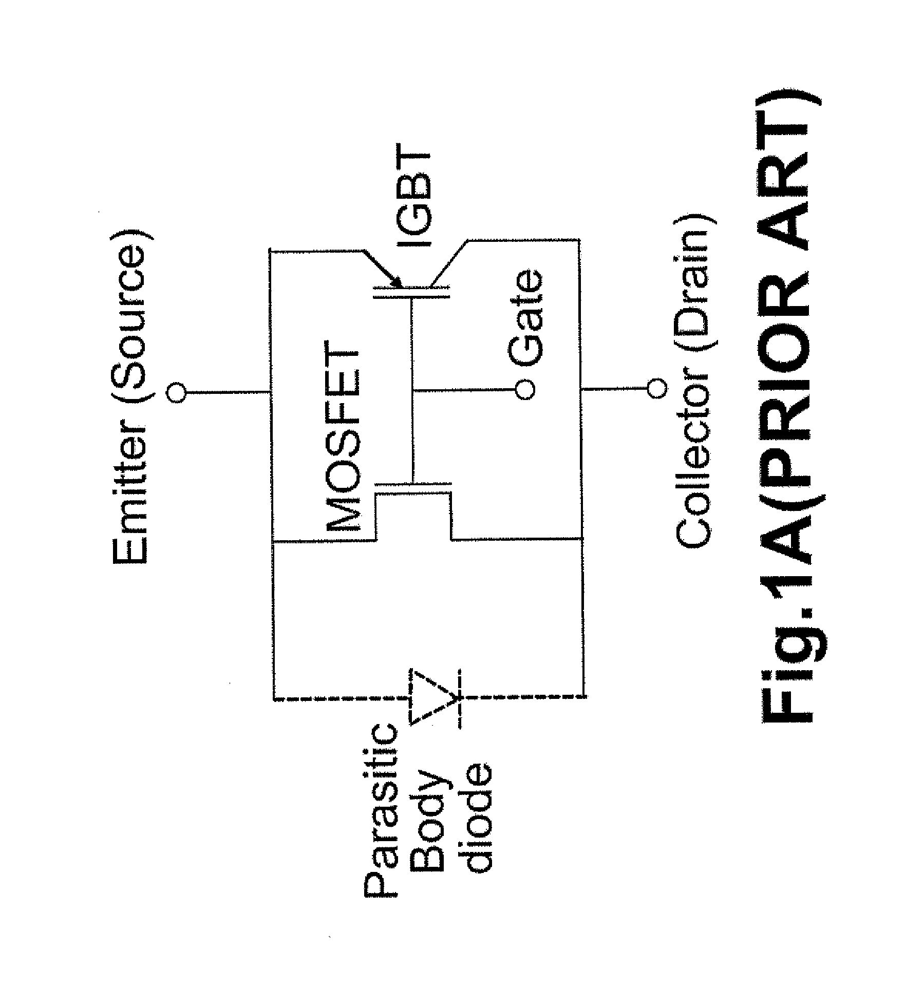
[0036]Please refer to FIG. 2 for an equivalent circuit of the present invention comprising a copacked trench IGBT with a trench MOSFET monolithically integrated with a Schottky diode in a same package, wherein the trench IGBT can be implemented by a trench PT IGBT or by a trench NPT IGBT. The equivalent circuit comprises an emitter node of the trench IGBT connected to a source node of the trench MOSFET and an anode node of the Schottky diode, a collector node of the trench IGBT connected to a drain node of the trench MOSFET and cathode node of the Schottky diode, and a gate node of the trench IGBT connected to that of the trench MOSFET.

[0037]Please refer to FIG. 3 for an equivalent circuit of the present invention comprising a copacked trench IGBT with a trench MOSFET monolithically integrated with a soft recovery diode in a same package, wherein the trench IGBT can be implemented by a trench PT IGBT or by a trench NPT IGBT.

[0038]Please refer to FIG. 4 for an equivalent circuit of t...


PUM


Abstract

A power semiconductor device comprising a trench IGBT, a trench MOSFET and a fast switching diode for reduction of turn-on loss is disclosed. The inventive semiconductor power device employs a fast switching diode instead of body diode in the prior art. Furthermore, the inventive semiconductor power device further comprises an additional ESD protection diode between emitter metal and gate metal.

Description

FIELD OF THE INVENTION[0001]This invention relates generally to the device configuration for fabricating the semiconductor power device. More particularly, this invention relates to an improved and novel device configuration for providing a power semiconductor power device comprising a trench IGBT (Insulation Gate Bipolar Transistor), trench MOSFET (Metal Oxide Semiconductor Field Effect Transistor) and fast switching diode for reduction of turn-on loss.BACKGROUND OF THE INVENTION[0002]FIG. 1A shows an equivalent circuit of a hybrid trench IGBT and trench MOSFET with a parasitic body diode for on-resistance reduction at Vice (Voltage between collector and emitter, similarly hereinafter) below 0.6V, please refer to the cross sectional view in FIG. 1B having a parasitic P+ body diode underneath each the trenched source-body contact which is disclosed in U.S. Pat No. 6,627,961.[0003]However, the P+ heavily doped parasitic body diode in the trench MOSFET has low switching speed and high...

Claims


Application Information

Patent Timeline
Patent Type & Authority Applications(United States)
IPC IPC(8): H01L23/58H01L29/74
CPCH01L29/0619H01L29/0649H01L29/7397H01L29/7804H01L29/7805H01L29/7806H01L29/7811H01L2924/0002H01L29/7813H01L29/861H01L29/8611H01L29/872H01L2924/00
Inventor HSIEH, FU-YUAN
Owner FORCE MOS TECH CO LTD
Why Eureka
Try Eureka