Semiconductor device and noise suppressing method
a technology of semiconductor devices and noise suppression, which is applied in the direction of semiconductor devices, semiconductor/solid-state device details, electrical apparatus, etc., can solve the problems of electromagnetic waves radiated from the connection member, become noise, etc., and achieve the effect of preventing a noise from leaking
- Summary
- Abstract
- Description
- Claims
- Application Information
AI Technical Summary
Benefits of technology
Problems solved by technology
Method used
Image
Examples
first embodiment
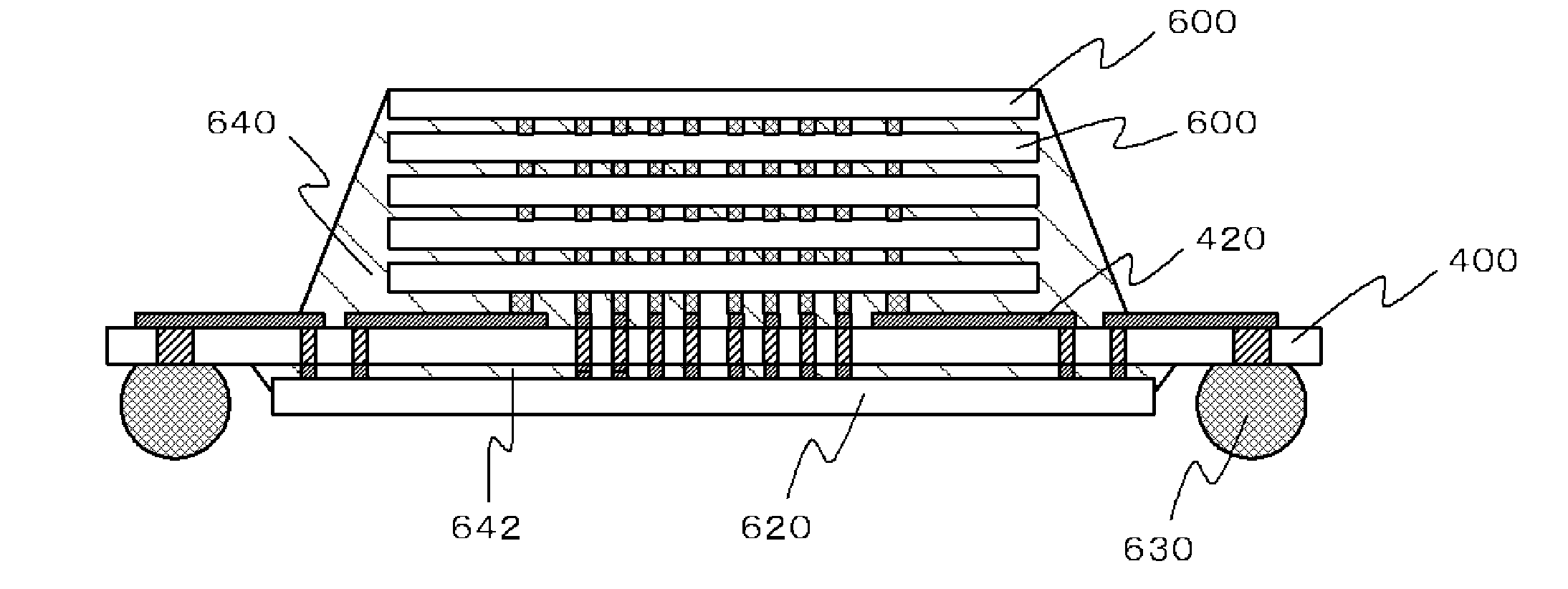
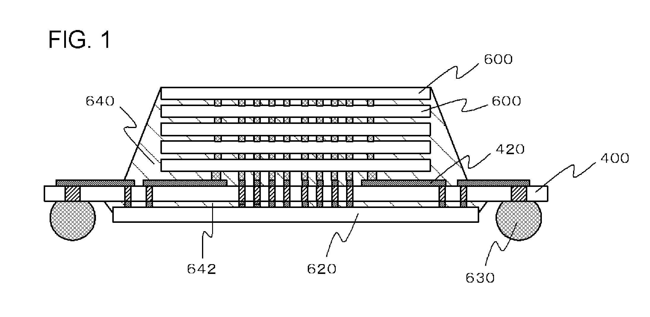
[0043]FIG. 1 shows a cross-sectional diagram illustrating a configuration of a semiconductor device according to a This semiconductor device includes an interposer substrate 400, a plurality of semiconductor chips 600, a semiconductor chip 620, and solder balls 630 serving as external connection terminals. The plurality of semiconductor chips 600 are memory chips and are stacked on one face of the interposer substrate 400. The semiconductor chip 620 is a system LSI, and is mounted on the other face of the interposer substrate 400. The plurality of semiconductor chips 600 and the semiconductor chip 620 overlap each other in a plan view.
[0044]The semiconductor chips 600 are stacked in a manner such that its active face, that is, a face on which an element such as a transistor, a multi-layer wiring, and a redistribution layer are formed faces an opposite direction with respect to the interposer substrate 400. Each of the semiconductor chips 600 has a through-via (shown in FIG. 2), and...
third embodiment
[0068]According to this embodiment, the same effect as the third embodiment may be obtained. Additionally, resistance of the lower-side conductor plane in the mushroom-type EBG structure may be made to be low. As a result, rising and falling of the band gap of the EBG structure 20 may be steepened.
[0069]FIG. 7 shows a cross-sectional diagram illustrating a configuration of a semiconductor device according to a fifth embodiment. This drawing corresponds to FIG. 2 in the first embodiment. The semiconductor device according to this embodiment has the same configuration as the semiconductor device according to the first embodiment except for the following aspects.
[0070]First, the first semiconductor chip 200 is provided with a conductor pattern 250 (third conductor) and an insulating layer 240. The conductor pattern 250 has a sheet shape and is formed on the insulating layer 210. The insulating layer 240 is formed on the conductor pattern 250. The plurality of island-shaped conductor pa...
second embodiment
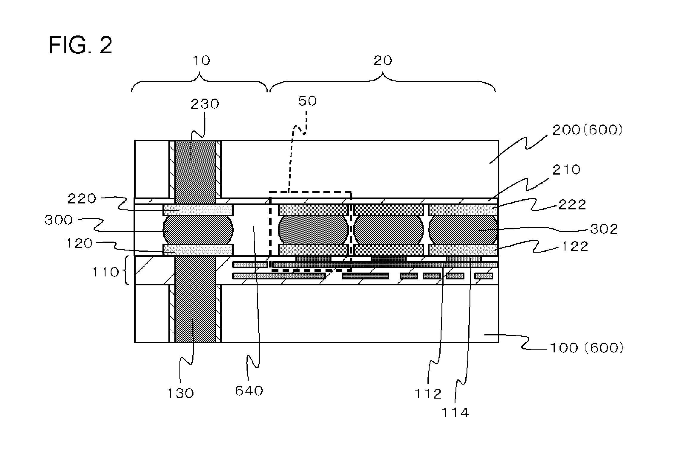
[0088]The EBG structure 20 in this embodiment does not include the vias 212 and the first conductor patterns 222. Instead, the EBG structure 20 includes the impurity region 202, second conductor patterns 122 cut into conductor pieces, and the vias 114. The configurations of the impurity region 202, the second conductor patterns 122 cut into conductor pieces, and the vias 114 are similar to those shown in FIG. 4 in the
[0089]This EBG structure 20 is a mushroom-type EBG structure, but the impurity region 202 corresponds to a conductor plane opposite to the head of the mushroom. The first conductor plane 112 corresponds to a conductor plane connected to the mushroom. The vias 114 correspond to an inductance portion of the mushroom. The second conductor patterns 122 cut into conductor pieces correspond to a head portion of the mushroom. The plurality of second conductor patterns 122 are electrically connected to each other through the plurality of vias 114 and the conductor pattern 112.
PUM
 Abstract
Description
Claims
Application Information
 - R&D
- Intellectual Property
- Life Sciences
- Materials
- Tech Scout
- Unparalleled Data Quality
- Higher Quality Content
- 60% Fewer Hallucinations
Browse by: Latest US Patents, China's latest patents, Technical Efficacy Thesaurus, Application Domain, Technology Topic, Popular Technical Reports.
© 2025 PatSnap. All rights reserved.Legal|Privacy policy|Modern Slavery Act Transparency Statement|Sitemap|About US| Contact US: help@patsnap.com


