Pfc converter
a converter and converter technology, applied in the field of pfc converters, can solve problems such as difficulty in reducing costs, and achieve the effect of reducing costs
- Summary
- Abstract
- Description
- Claims
- Application Information
AI Technical Summary
Benefits of technology
Problems solved by technology
Method used
Image

Examples
first preferred embodiment
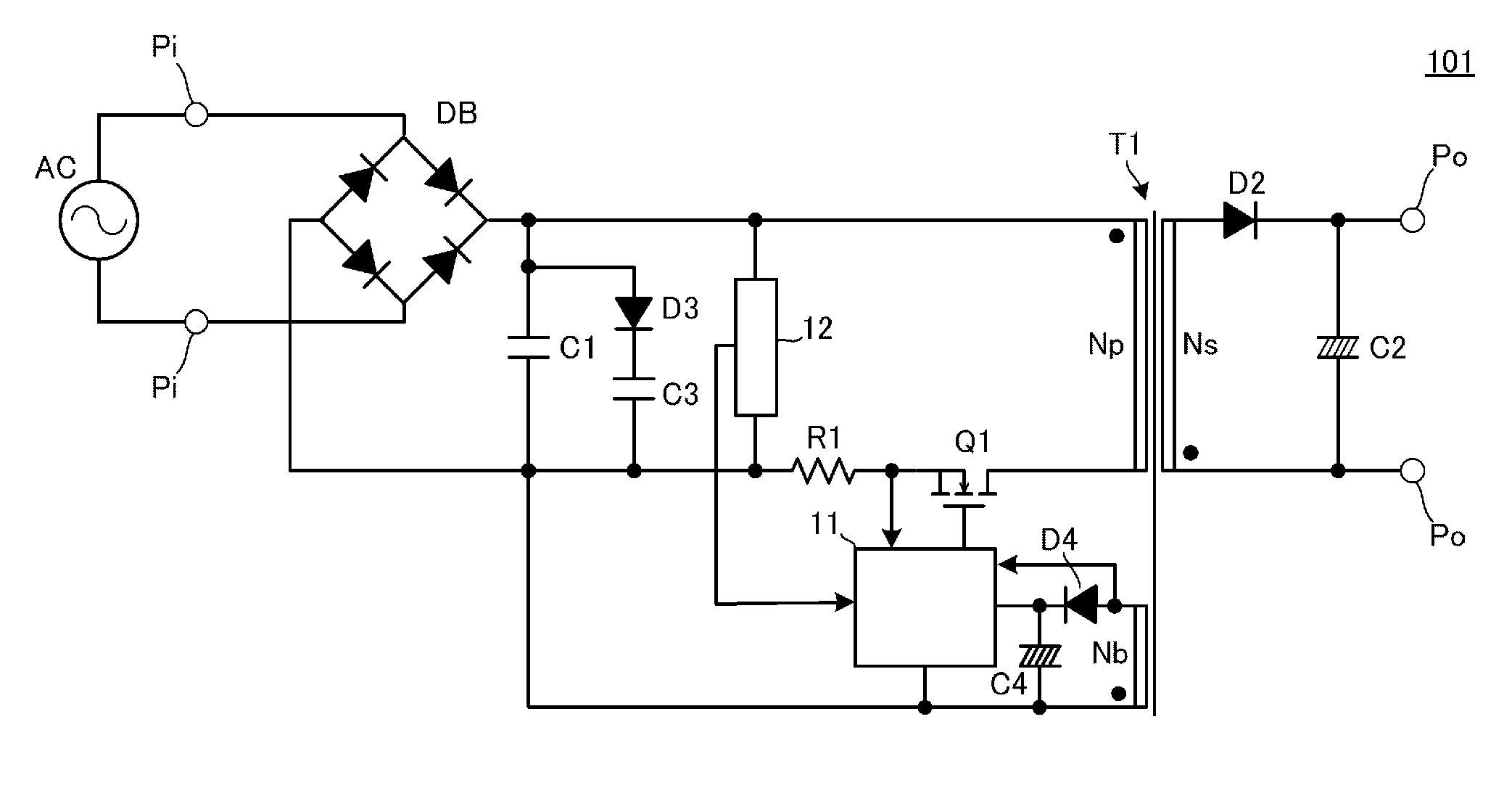
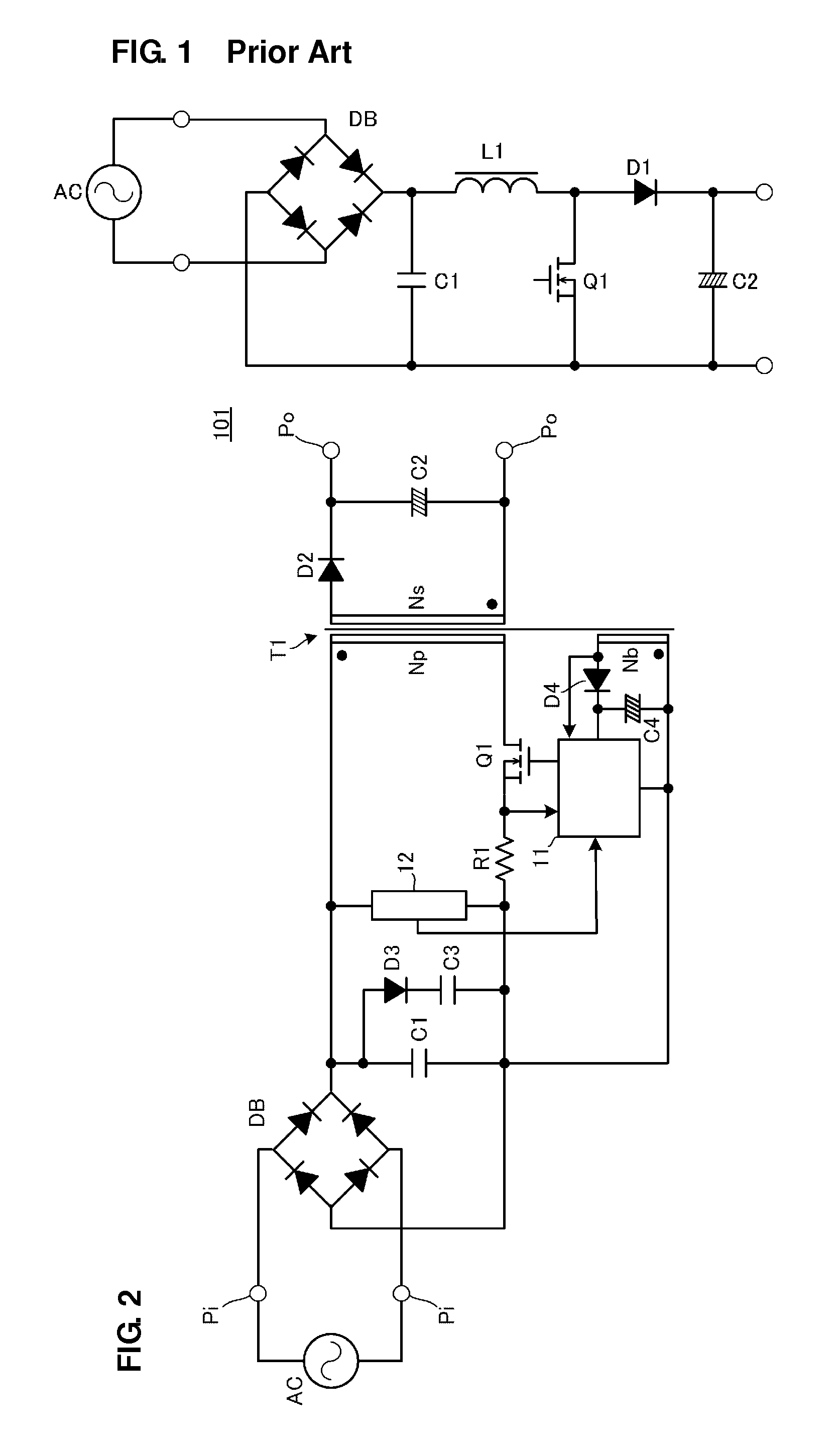
[0033]FIG. 2 is a circuit diagram of a PFC converter 101 according to the first preferred embodiment of the present invention.
[0034]In the PFC converter 101, a commercial alternating-current power supply preferably is connected to input terminals Pi and a load is connected to output terminals Po. This load is, for example, an LED included in an LED illumination apparatus.
[0035]A diode bridge DB that is a rectifying circuit is connected to the input terminals Pi. A first series circuit including a primary winding Np of a transformer T1 and a switching element Q1 is connected to an output portion of the diode bridge DB. A filter capacitor C1 is connected to the output portion of the diode bridge DB. A rectifying and smoothing circuit including a rectifier diode D2 and a smoothing capacitor C2 is connected to a secondary winding Ns of the transformer T1.
[0036]A second series circuit including a diode D3 and a second capacitor C3 connected in series to each other is connected in paralle...
second preferred embodiment
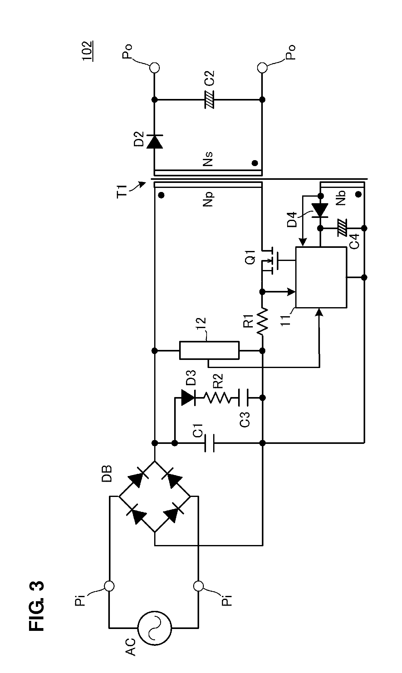
[0043]FIG. 3 is a circuit diagram of a PFC converter 102 according to a second preferred embodiment of the present invention.
[0044]The difference between the PFC converter 102 and the PFC converter 101 according to the first preferred embodiment illustrated in FIG. 2 is that the second series circuit connected in parallel to the filter capacitor C1 includes the diode D3, the second capacitor C3, and a resistor R2 connected in series to one another.
[0045]Since the resistor R2 is connected in series to the charging path for the capacitor C3, the peak of a charging current applied to the capacitor C3 can be limited even when the capacitance of the capacitor C3 is increased. Accordingly, elements such as the diode bridge DB and the diode D3 on the charging current path do not need to have a high rated current. This leads to cost reduction.
third preferred embodiment
[0046]FIG. 4 is a circuit diagram of a PFC converter 103 according to a third preferred embodiment of the present invention.
[0047]The difference between the PFC converter 103 and the PFC converter 101 according to the first preferred embodiment illustrated in FIG. 2 is that a resistor R3 is connected in parallel to the capacitor C3.
[0048]The resistor R3 aggressively forms a discharging path of an electrical charge stored in the capacitor C3. An electrical charge stored in the capacitor C3 at the time of connection to the commercial alternating-current power supply AC is rapidly discharged at the time of disconnection from the commercial alternating-current power supply AC. Accordingly, even when the commercial alternating-current power supply AC is intermittently connected and disconnected to and from the input terminals Pi of the PFC converter 103 in a short period, a predetermined charging current flows through the capacitor C3. The effect of reducing a superimposed current is the...
PUM
 Abstract
Description
Claims
Application Information
 - R&D
- Intellectual Property
- Life Sciences
- Materials
- Tech Scout
- Unparalleled Data Quality
- Higher Quality Content
- 60% Fewer Hallucinations
Browse by: Latest US Patents, China's latest patents, Technical Efficacy Thesaurus, Application Domain, Technology Topic, Popular Technical Reports.
© 2025 PatSnap. All rights reserved.Legal|Privacy policy|Modern Slavery Act Transparency Statement|Sitemap|About US| Contact US: help@patsnap.com