Manufacturing method for monolithic ceramic electronic component

a manufacturing method and electronic component technology, applied in capacitor manufacture, lamination printed circuit boards, fixed capacitor details, etc., can solve the problems of increasing the risk of short-circuit, so as to reduce the possibility of unwanted external force, reduce the chance of short-circuit, and reduce the distance between internal electrodes of different polarities

Active Publication Date: 2012-09-20
MURATA MFG CO LTD
View PDF9 Cites 48 Cited by
  • Summary
  • Abstract
  • Description
  • Claims
  • Application Information

AI Technical Summary

Benefits of technology

[0027]According to a preferred embodiment of the present invention mentioned above, in handling the green chips arrayed in the row and column directions or the rod-shaped green block bodies arrayed in the predetermined direction which are obtained by cutting the mother block, the tumbling step is performed which includes tumbling the green chips or the rod-shaped green block bodies in a state in which the arrayed green chips or rod-shaped green block bodies are spaced apart from each other, thereby making the cut side surface of each of the green chips or the rod-shaped green block bodies uniformly an open surface. Thus, it is possible to reduce the possibility of unwanted external force being exerted on the cut side surface of the green chip or the rod-shaped green block body. Therefore, it is possible to reduce the chances of short-circuiting, even when the stacking ceramic green sheets become thinner and therefore the distance between internal electrodes of different polarities decreases.
[0028]According to the preferred embodiments of the present invention mentioned above, the affixing step, which includes affixing the side surface ceramic green sheet to the cut side surface of the green chip that has become an open surface to thereby form a raw ceramic protective layer, is performed simultaneously for each of a plurality of green chips arrayed in the row and column directions and whose cut side surface is uniformly oriented so as to become an open surface. Thus, as in the case of performing the affixing step for the rod-shaped green block body, the af...

Problems solved by technology

However, reducing the dimensions of the protective area 6 at the end undesirably increases the risk of short-circuiting of the first external electrode and the second external electrode via either one of the internal electrodes 1 and 2.
However, the technique described in Japanese Unexamined Patent Application Publication No. 6-349669 mentioned above has the following problems.
Therefore, in handling the green chips, an unwanted short-circuit may occur between the internal electrodes with different polarities unless utmost attention is paid to the handling of their side surfaces.
In particular, as stacking ceram...

Method used


Image

  • Manufacturing method for monolithic ceramic electronic component
  • Manufacturing method for monolithic ceramic electronic component
  • Manufacturing method for monolithic ceramic electronic component

Examples


Embodiment Construction

[0053]Hereinafter, preferred embodiments of the present invention are described, with a monolithic ceramic capacitor taken as a non-limiting example of monolithic ceramic electronic component.

[0054]FIGS. 1 to 16 illustrate a first preferred embodiment of the present invention.

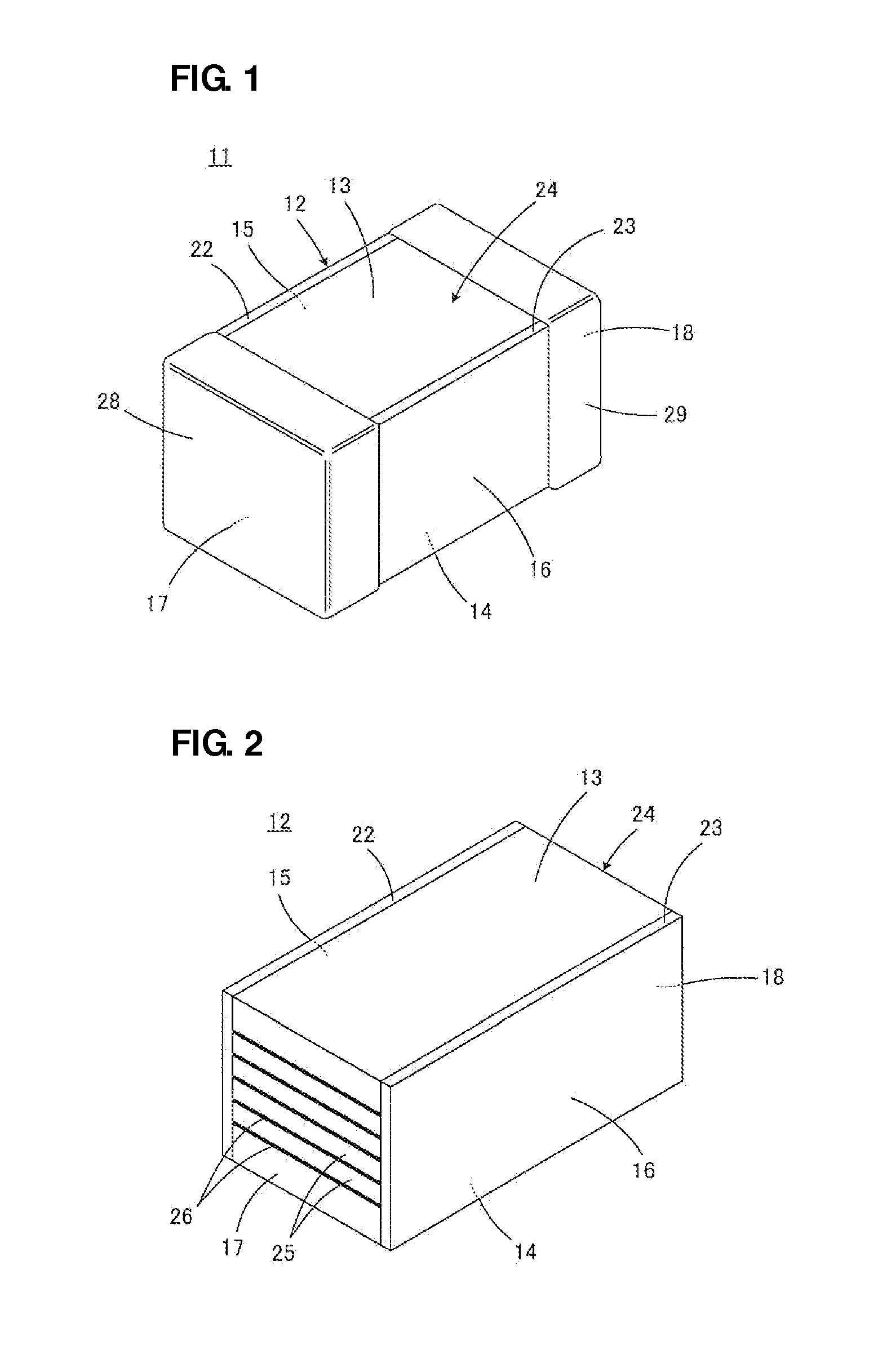
[0055]First, as illustrated in FIG. 1, a monolithic ceramic capacitor 11 includes a component body 12. The component body 12 is illustrated singly in FIG. 2. The component body 12 preferably has a rectangular parallelepiped or substantially rectangular parallelepiped shape including a pair of opposing principal surfaces 13 and 14, a pair of opposing side surfaces 15 and 16, and a pair of opposing first and second end surfaces 17 and 18.

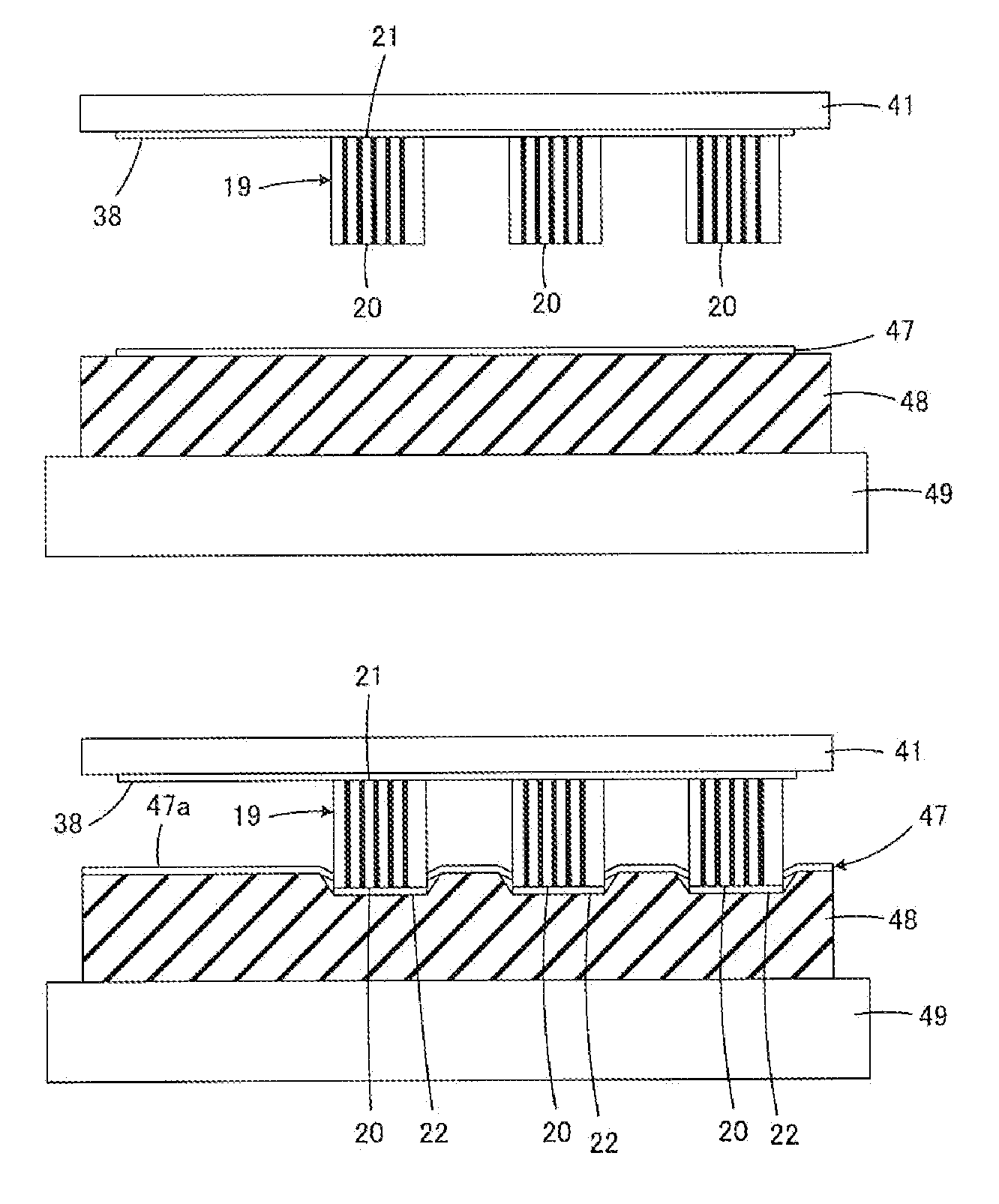
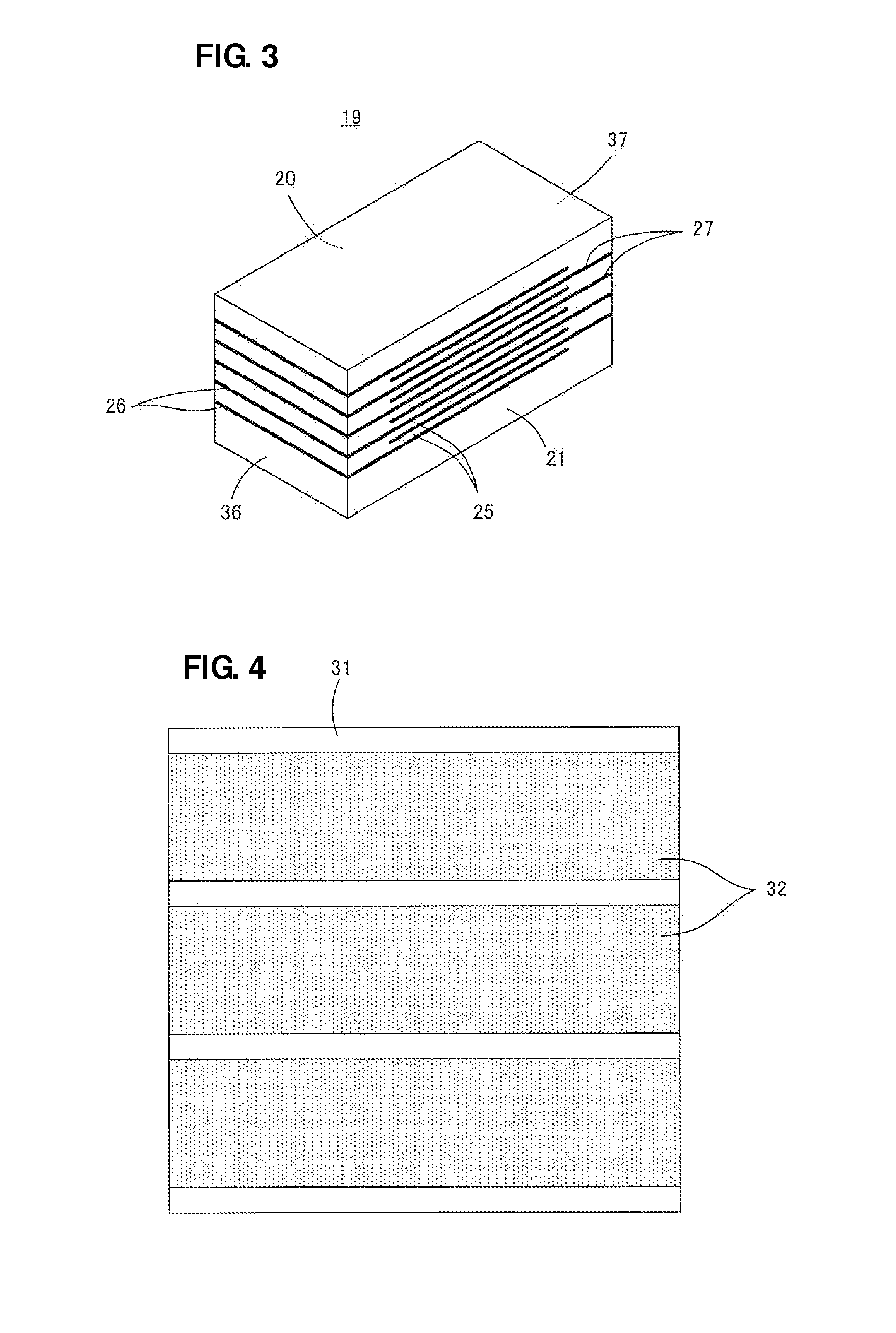
[0056]In describing the component body 12 in detail, reference is also made to FIG. 3 illustrating the outward appearance of a green chip 19 prepared to obtain the component body 12. As will be appreciated from a description given later, the component body 12 corresponds to a com...


PUM

PropertyMeasurementUnit
Temperatureaaaaaaaaaa
Forceaaaaaaaaaa
Adhesion strengthaaaaaaaaaa

Abstract

In a manufacturing method for a monolithic ceramic electronic component, a plurality of green chips arrayed in row and column directions which are obtained after cutting a mother block are spaced apart from each other and then tumbled, thereby uniformly making the side surface of each of the green chips an open surface. Thereafter, an adhesive is applied to the side surface. Then, by placing a side surface ceramic green sheet on an affixation elastic body, and pressing the side surface of the green chips against the side surface ceramic green sheet, the side surface ceramic green sheet is punched and stuck to the side surface.

Description

BACKGROUND OF THE INVENTION[0001]1. Field of the Invention[0002]The present invention relates to a manufacturing method for a monolithic ceramic electronic component, and more specifically, to a method for forming a protective area at the side of internal electrodes in a monolithic ceramic electronic component.[0003]2. Description of the Related Art[0004]A monolithic ceramic capacitor exists as an example of a monolithic ceramic electronic component to which the present invention is directed. To manufacture a monolithic ceramic capacitor, typically, a step as illustrated in FIGS. 21A and 21B is performed. That is, a first ceramic green sheet 3 on which a first internal electrode 1 is formed, and a second ceramic green sheet 4 on which a second internal electrode 2 is formed are alternately stacked in a plurality of layers. A raw component body is obtained by this stacking step. After the raw component body is fired, first and second external electrodes are formed on opposing first a...

Claims


Application Information

Patent Timeline
IPC IPC(8): B32B37/14B02C19/00
CPCH01G4/12H01G4/30H01G13/00Y10T156/1052B32B37/10B32B37/00H05K3/0058H01L21/64Y10T156/1348B26D1/04B32B37/02B32B37/12B32B37/16B32B38/0004B32B38/04B32B2038/042C04B35/00C04B35/468C04B37/00C04B37/006C04B2237/12C04B2237/32H01G4/06H01G4/308
Inventor MATSUI, TOGODOOKA, MINORUTAKASHIMA, HIROYOSHIOKAJIMA, KENICHI
Owner MURATA MFG CO LTD
Why Eureka
Try Eureka