Thermal-type infrared solid-state image sensing device and method of manufacturing the same

a solid-state image and sensing device technology, applied in the direction of optical radiation measurement, instruments, material analysis, etc., can solve the problems of inability to accurately detect the temperature of an object, complicated device structure, and high cost of the device, so as to improve improve the heat transfer effect of discharging heat with good efficiency, and increase the residual stress reduction

Active Publication Date: 2012-09-27
NEC CORP
View PDF1 Cites 2 Cited by
  • Summary
  • Abstract
  • Description
  • Claims
  • Application Information

AI Technical Summary

Benefits of technology

[0046]In the thermal-type infrared solid-state image sensing device of the present invention, the reference element is such that the slit which forms the light receiving section in the insulating film (protective film) which comprises the thermoelectric conversion element in the interior thereof is opened up to the sacrifice layer, at least one or more layers of films of electrically conductive material which cover at least the light receiving section and the slit section are provided, and the protective film is further provided above at least the slit on the film of electrically conductive material. Therefore, it is possible to realize such configuration that the sacrifice layer of the reference element is protected and remains also during etching for forming of the hollow section by removing the sacrifice layer of the light receiving element. Although in the slit of the reference element, there are the film of electrically conductive material without a slit and the protective film thereon, they enter the slit along the side wall of the slit and a void remains within the slit. Therefore, the effect of providing the slit is kept as it is. The film of electrically conductive material is present between the insulating film (protective film) including the thermoelectric conversion element in the interior thereof and the protective film on the film of electrically conductive material and serves as a buffer material between the two protective films. Therefore, it is possible to increase the residual stress reducing effect compared to the direct contact of the protective films. Furthermore, the light blocking effect against incident infrared rays is improved by the film of electrically conductive material and in addition, the heat transfer effect of dissipating heat with good efficiency is also improved.
[0047]If this film of electrically conductive material is a stacked film of a material film having a relatively good step coverage and a material film having a relatively bad step coverage, it is possible to positively achieve electrical stabilization by a constant potential to the whole film of electrically conductive material through the use of the material film having a relatively good step coverage which coats the side wall of the slit and it is possible to realize the configuration in which the void is caused to remain in the slit even when the light blocking effect is increased by increasing the film thickness of the surface layer through the use of the material film having a relatively bad step coverage which is stacked.
[0048]And in the case of the adoption of the configuration in which the protective film on the film of electrically conductive material is removed in a predetermined region on the light *receiving section or on the supporting section formed in the same level as the light receiving section, it is possible to reduce the residual stresses of the protective material itself on the film of electrically conductive material.
[0049]Furthermore, the method of manufacturing a thermal-type infrared solid-state image sensing device of the present invention comprises at least the step of forming a slit which pierces through the insulating film (protective film) which comprises a thermoelectric conversion element in the interior thereof only in the reference section after manufacture before the formation of slits forming the light receiving element and the light receiving section of the reference element by a conventional method, the step of forming a film of electrically conductive material and forming a protective film after the removal of the film of electrically conductive material except at least the area on the reference section and the slit, the step of forming a slit which pierces through the insulating film (protective film) which comprises a thermoelectric conversion element in the interior thereof only in the image sensing section, and the step of removing the sacrifice layer of the image sensing section via the slit of the image sensing section, whereby it is possible to realize the manufacture of the thermal-type infrared solid-state image sensing device of the present invention having the above-described configuration.

Problems solved by technology

A thermoelectric conversion element, such as a bolometer, detects the intensity of infrared rays by a temperature change caused by the infrared rays which are absorbed, and hence if the environmental temperature and the like change, a drift occurs in the thermal-type infrared solid-state image sensing device, with the result that it becomes impossible to accurately detect the temperature of an object.
However, in this method, it is necessary to separately provide a temperature controller and this complicates the structure of the device and makes the device expensive.
In a light receiving element provided with a light receiving section (temperature detection section) and a supporting section in the same hierarchical layer, the area capable of being allotted to the supporting section decreases if the area of the light receiving section (temperature detection section) is increased, whereas contrastingly the area of the light receiving section (temperature detection section) is reduced if the area occupied by the supporting section is increased; this is unfavorable for downsizing.
However, a decrease in the area of the light receiving section (temperature detection section) reduces the “bolometer thin film volume,” causing an increase in 1 / f noise.
That is, a decrease in the S / N ratio caused by an increase in 1 / f noise occurs.

Method used


Image

  • Thermal-type infrared solid-state image sensing device and method of manufacturing the same
  • Thermal-type infrared solid-state image sensing device and method of manufacturing the same
  • Thermal-type infrared solid-state image sensing device and method of manufacturing the same

Examples


first exemplary embodiment

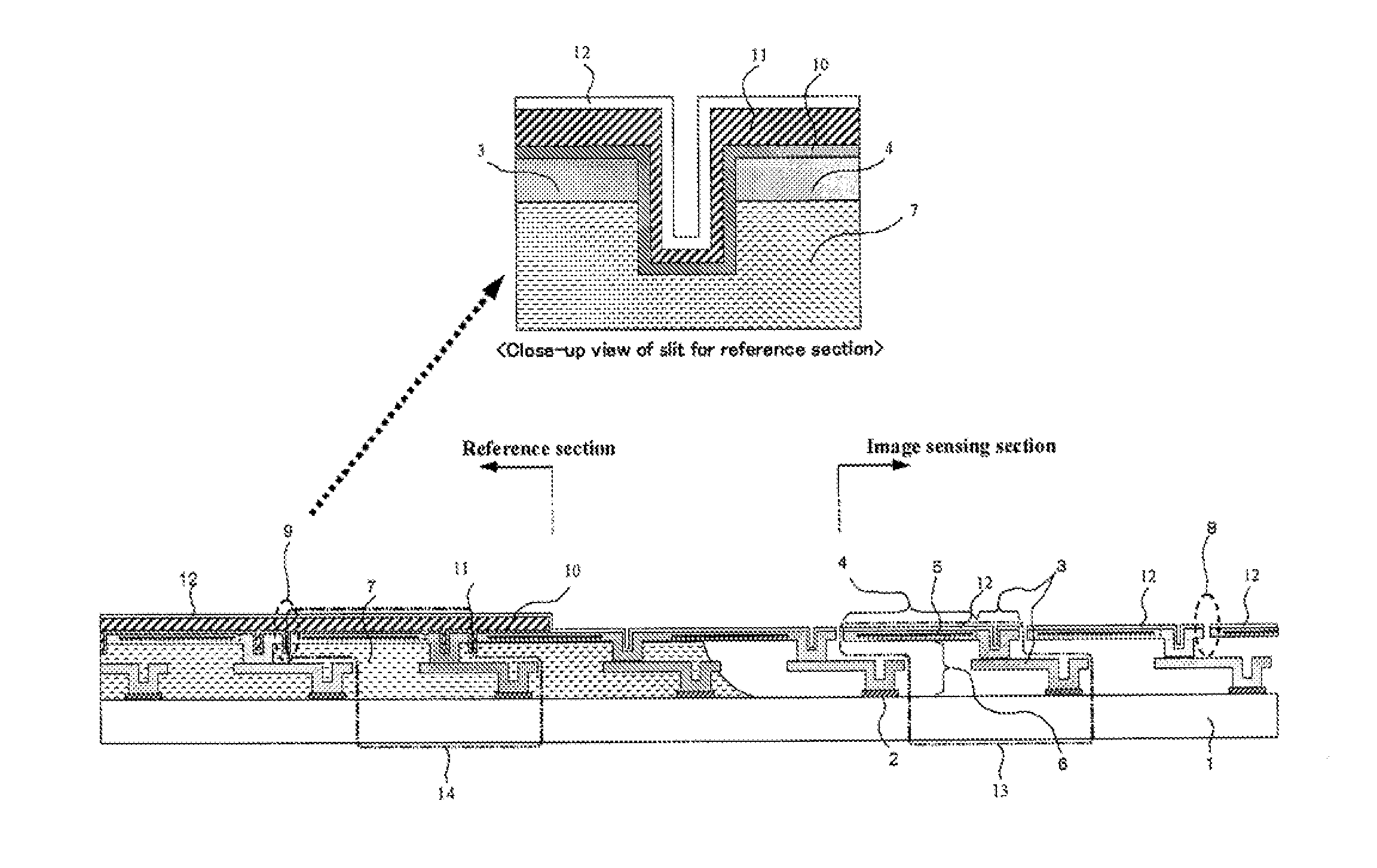
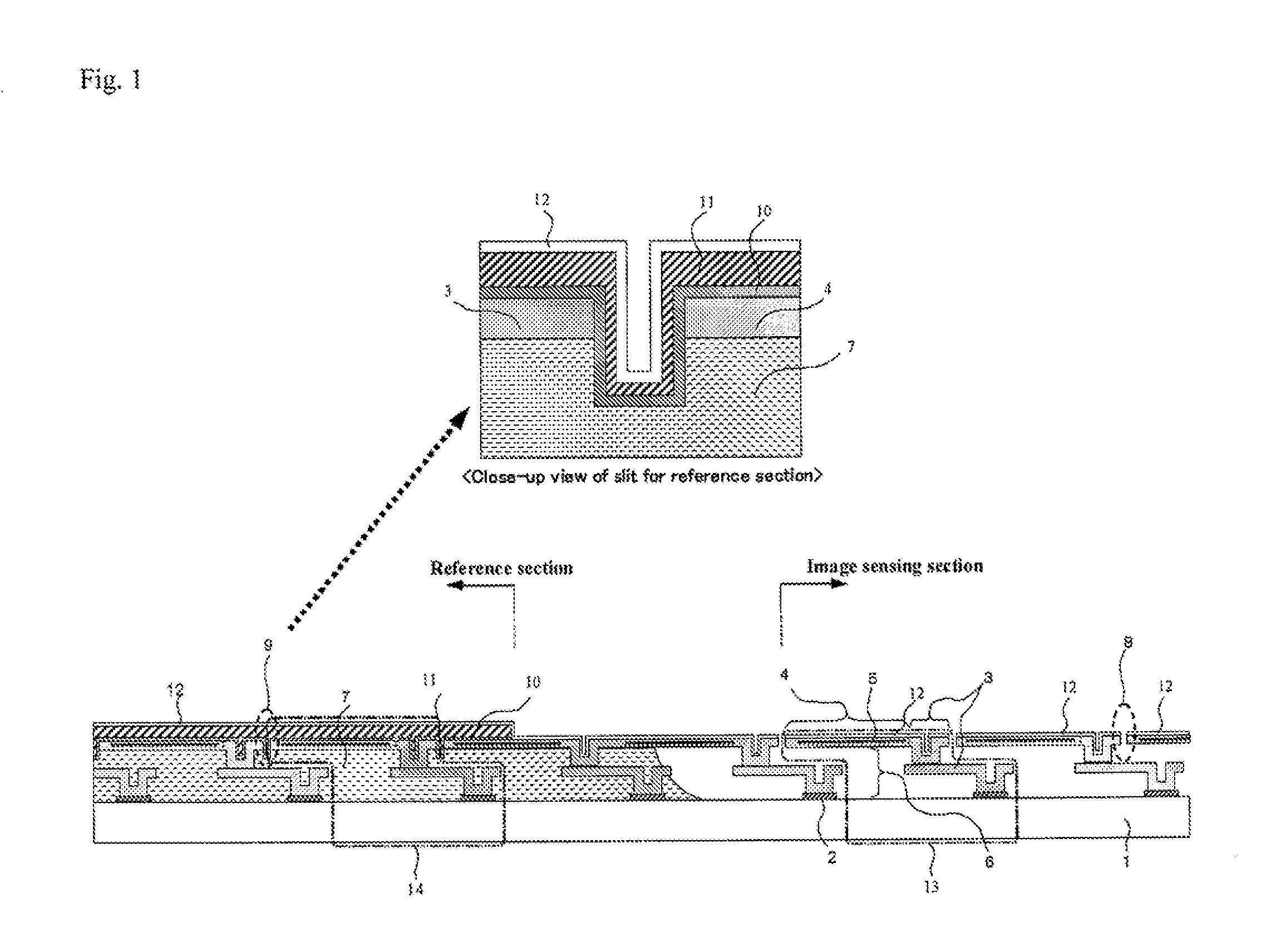
[0149]Experimentally produced was a thermal-type infrared solid-state image sensing device which has effective 640×480 light receiving pixels in an image sensing section and is provided with a couple of reference sections having reference pixels in eight rows, which are respectively positioned above and below the image sensing section in its vertical direction. The slit widths of the image sensing section slit and the reference section slit are 0.5 μm. The film thickness of the surface layer of the light blocking Ti film was set to 50 nm, the film thickness of the surface layer of the light blocking Al film was set to 250 nm, and the film thickness of the surface layer of the SiN film for protecting the film made of light blocking electrically conductive material or the sacrifice layer was set to 50 nm. The film thickness of the surface layer of the above-described light blocking Ti film, light blocking Al film and protective SiN film with respect to the slit width of the reference ...


PUM


Abstract

In the reference element employed in the thermal-type infrared solid-state image sensing device according to the present invention, a slit used for construction of a light receiving element is opened in insulating films between which a thermoelectric conversion element is tucked to such an extent that the slit pierces into the sacrifice layer; a film made of electrically conductive material covering the light receiving section and the slit is provided and a protective film is provided thereon, and the film made of electrically conductive material and the protective film enter the interior of the slit along a side wall of the slit, whereby a void is left in the interior of the slit. As a result, residual stresses of the insulating films are kept equal in the light receiving element and the reference element, and thereby, the light blocking effect and the heat transfer effect are improved.

Description

TECHNICAL FIELD [0001]The present invention relates to a thermal-type infrared solid-state image sensing device and a method of manufacturing the thermal-type infrared solid-state image sensing device and, more particularly, to a thermal-type infrared solid-state image sensing device provided with an image sensing section which detects infrared images and a reference section which outputs reference signals based on the environmental temperature and the like, and a method of manufacturing the thermal-type infrared solid-state image sensing device.BACKGROUND ART [0002]A thermal-type infrared solid-state image sensing device has a plurality of light receiving elements which are arranged in array. Each of the light receiving elements absorbs the infrared rays radiated from an object by use of a light receiving section (diaphragm) having microbridge structure, converts the infrared rays into heat, detects a temperature rise due to the heat by use of a thermoelectric conversion element, s...

Claims


Application Information

Patent Timeline
Patent Type & Authority Applications(United States)
IPC IPC(8): G01J5/12H01L31/18
CPCG01J5/12G01J2005/068H01L31/1876G01J5/024H01L27/1467G01J5/064
Inventor TOHYAMA, SHIGERU
Owner NEC CORP
Why Eureka
Try Eureka