Low capacitance transient voltage suppressor

a transient voltage and low capacitance technology, applied in the field of transient voltage suppressors, can solve the problems of large input capacitance, reducing the input capacitance of tvs devices without reducing device size, and affecting the operation of electronics, so as to reduce the breakdown voltage of bjt structure, reduce the resistance path, and reduce the input capacitance of i/o pins.

Active Publication Date: 2012-09-27
AMAZING MICROELECTRONICS
View PDF2 Cites 33 Cited by
  • Summary
  • Abstract
  • Description
  • Claims
  • Application Information

AI Technical Summary

Benefits of technology

[0008]A primary objective of the present invention is to provide a transient voltage suppressor, which uses an N-type heavily doped well to provide a low resistance path, wher

Problems solved by technology

Without suitable protection devices, the functions of these electronics could be reset or even damaged under ESD (Electrostatic Discharge) events.
However, the TVS device size should be designed large for better ESD performance which causes the large input capa

Method used


Image

  • Low capacitance transient voltage suppressor
  • Low capacitance transient voltage suppressor
  • Low capacitance transient voltage suppressor

Examples


first embodiment

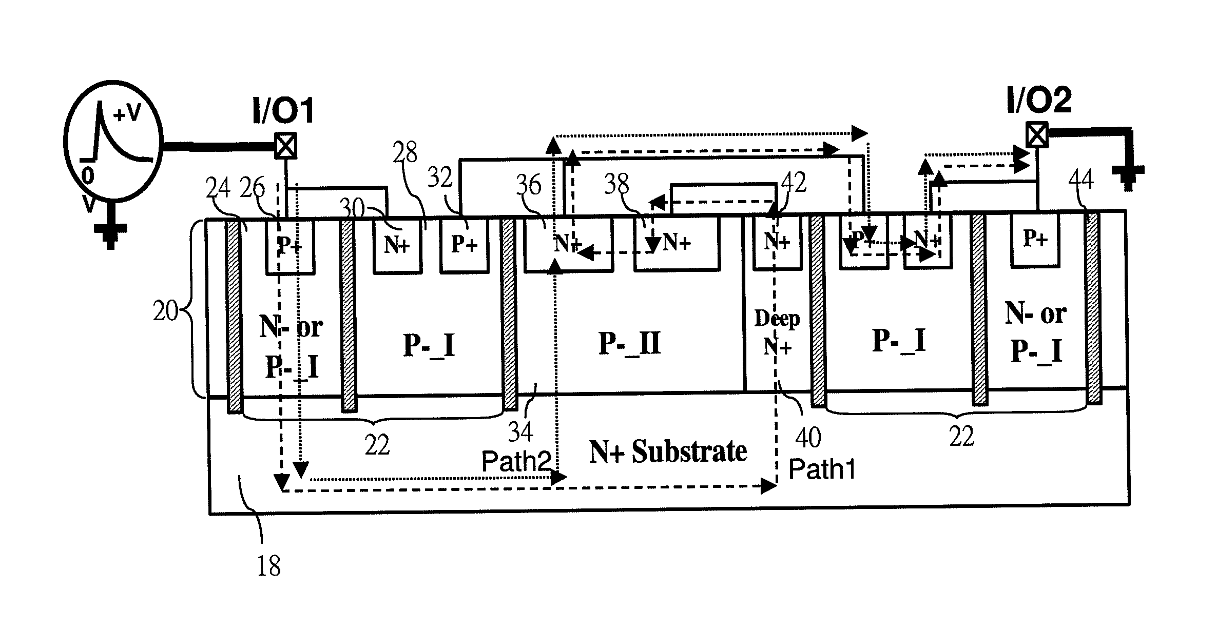
[0020]Refer to FIG. 4. With the fourth N-type heavily doped area 42 and the N-type heavily doped well 40, a low resistance path from the epitaxial surface to the N-type heavily doped substrate 18 is formed. As a result, the breakdown region occurs at the junction of the third N-type heavily doped area 38 and the second P-type lightly doped well 34. In other words, the breakdown voltage of lateral BJT can be easily adjusted to be smaller than that of vertical BJT. Therefore, the breakdown voltage of the present invention can be easily controlled as compared with that of prior art design. From FIG. 5, it is known that there are two ESD discharging paths in the For the I / O pin under positive ESD stress, the ESD current of path1 is discharged through the lateral BJT, and then discharged through the lateral diode to the grounded pin GND. The ESD current of path2 is discharged through the vertical BJT, and then discharged through the lateral diode to the grounded pin GND. With two ESD di...

second embodiment

[0022]According to the above-mentioned, each steering diode structure 22 has a lateral diode and a vertical diode. For describing the operation of the second embodiment in detail, the lateral diode and the vertical diode in the left side are respectively viewed as a first lateral diode and a first vertical diode, and the lateral diode and the vertical diode in the right side are respectively viewed as a second lateral diode and a second vertical diode.

[0023]Refer to FIG. 7. The operation of the second embodiment is similar to that of the first embodiment. As a result, the breakdown region also occurs at the junction of the third N-type heavily doped area 38 and the second P-type lightly doped well 34. In other words, the breakdown voltage of lateral BJT can be easily adjusted to be smaller than that of vertical BJT. Therefore, the breakdown voltage of the present invention can be easily controlled as compared with that of prior art design. From FIG. 7, it is known that there are two...


PUM


Abstract

A low capacitance transient voltage suppressor is disclosed. The suppressor comprises an N-type heavily doped substrate and an epitaxial layer formed on the substrate. At least one steering diode structure formed in the epitaxial layer comprises a diode lightly doped well and a first P-type lightly doped well, wherein a P-type heavily doped area is formed in the diode lightly doped well and a first N-type heavily doped area and a second P-type heavily doped area are formed in the first P-type lightly doped well. A second P-type lightly doped well having two N-type heavily doped areas is formed in the epitaxial layer. In addition, an N-type heavily doped well and at least one deep isolation trench are formed in the epitaxial layer, wherein the trench has a depth greater than or equal to depths of all the doped wells, so as to separate at least one doped well.

Description

BACKGROUND OF THE INVENTION[0001]1. Field of the Invention[0002]The present invention relates to a transient voltage suppressor, particularly to a low capacitance transient voltage suppressor.[0003]2. Description of the Related Art[0004]Because the IC device sizes have been shrunk to nanometer scale, the consumer electronics, like the laptop and mobile devices, have been designed to be much smaller than ever. Without suitable protection devices, the functions of these electronics could be reset or even damaged under ESD (Electrostatic Discharge) events. Currently, all consumer electronics are expected to pass the ESD test requirement of IEC 61000-4-2 standard. TVS (Transient Voltage Suppressor) is generally designed to bypass the ESD energy, so that the electronic systems can be prevented from ESD damages. The working principle of TVS is shown in FIG. 1. In FIG. 1, the TVS devices 10 are connected in parallel with the protected circuits 12 on the PCB (Printed Circuit Board). These T...

Claims


Application Information

Patent Timeline
IPC IPC(8): H01L29/66
CPCH01L29/861H01L27/0255
Inventor SHEN, YU-SHULIN, KUN-HSIENCHUANG, CHE-HAOJIANG, RYAN HSIN-CHIN
Owner AMAZING MICROELECTRONICS
Why Eureka
Try Eureka