Metrology Method and Apparatus, and Device Manufacturing Method

a metrology and manufacturing method technology, applied in the direction of photomechanical apparatus, instruments, printers, etc., can solve the problems of inability to assume the optical system, the apparatus is potentially more complex, and the process is slow

Active Publication Date: 2012-09-27
ASML NETHERLANDS BV
View PDF3 Cites 484 Cited by
  • Summary
  • Abstract
  • Description
  • Claims
  • Application Information

AI Technical Summary

Benefits of technology

[0009]It is desirable to provide a method and apparatus for dark field metrology, for example to measure asymmetry

Problems solved by technology

On the other haul, the requirement to rotate the target, which may be on a large substrate, makes the process slow and the apparatus potentially more complex.
Also, if the target after rotation is not positioned exactly where it was measured before, it cannot be assumed that the optical system will perform exactly the same in both measurements.
Accurate positioning requires mo

Method used


Image

  • Metrology Method and Apparatus, and Device Manufacturing Method
  • Metrology Method and Apparatus, and Device Manufacturing Method
  • Metrology Method and Apparatus, and Device Manufacturing Method

Examples


first embodiment

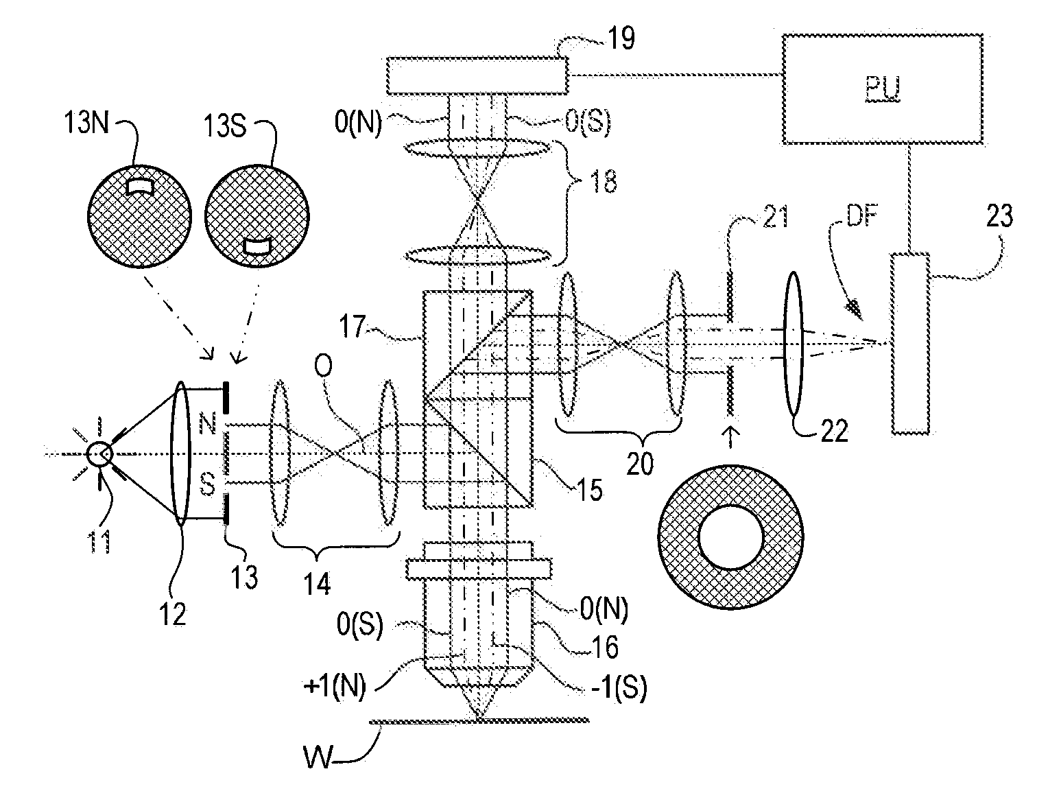
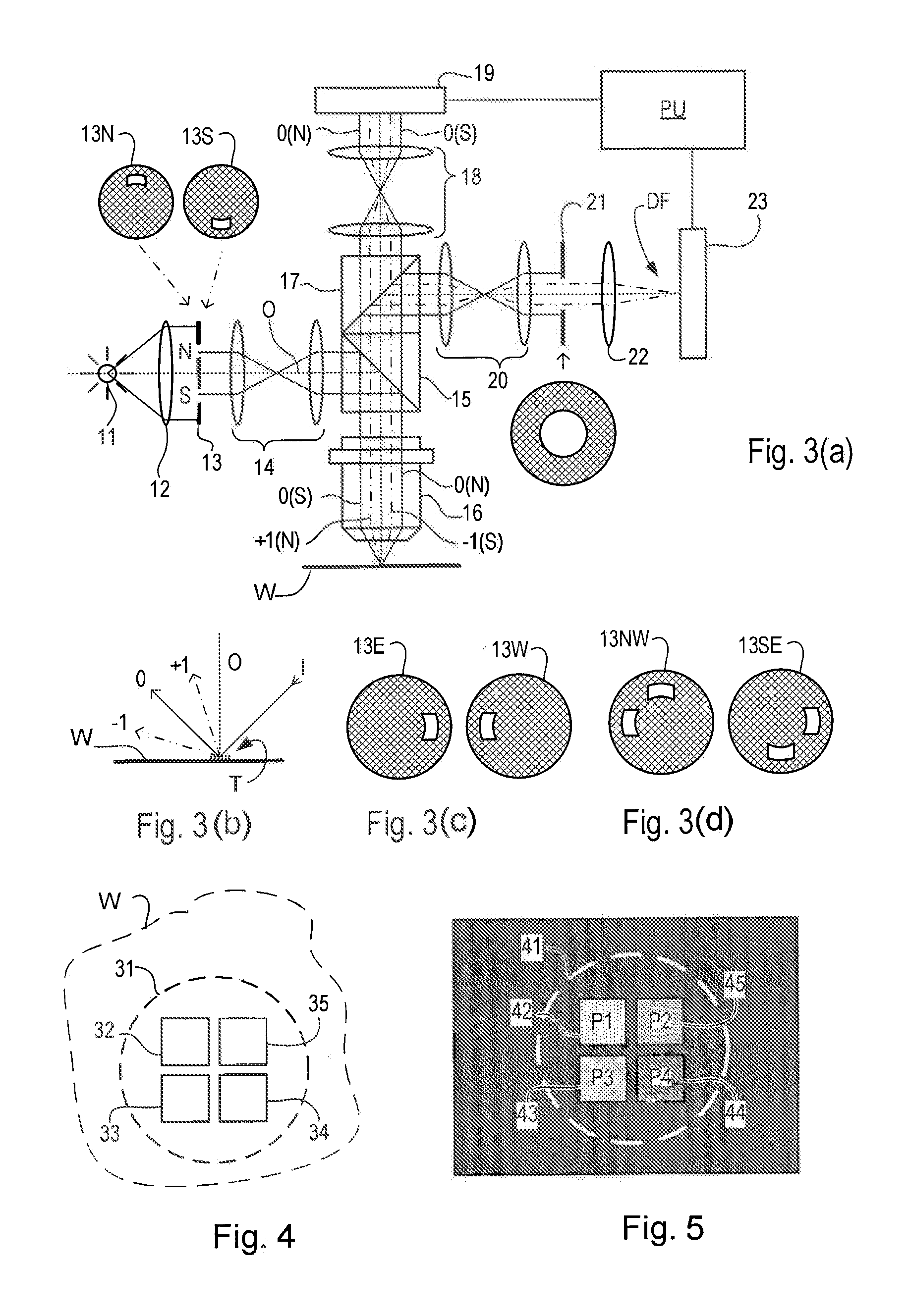
[0010]the present invention provides a method of measuring asymmetry in a periodic structure formed by a lithographic process on a substrate, the method comprising the steps of: using the lithographic process to form a periodic structure on the substrate, a first measurement step comprising forming and detecting a first image of the periodic structure while illuminating the structure with a first beam of radiation, the first image being formed using a first part of non-zero order diffracted radiation while excluding zero order diffracted radiation, a second measurement step comprising forming and detecting a second image of the periodic structure while illuminating the structure with a second beam of radiation, the second image being formed using a second part of the non-zero order diffracted radiation which is symmetrically opposite to the first part, in a diffraction spectrum of the periodic structure, and using a difference in intensity values derived from the detected first and ...

second embodiment

[0013]the present invention further provides an inspection apparatus configured for measuring asymmetry in a periodic structure on a substrate, the inspection apparatus comprising: an illumination arrangement operable to deliver first and second beams of radiation to the substrate for use in first and second measurement steps, a detection arrangement operable during the first and second measurement steps to form and detect respective first and second images of the substrate using radiation diffracted from the substrate, and a stop arrangement within the detection arrangement. The illumination arrangement and stop arrangement together are effective to stop zero order diffracted radiation contributing to the first and second images, and are configurable to form first and second images using first and second parts respectively of the non-zero order diffracted radiation, the first and second parts being symmetrically opposite one another in a diffraction spectrum of the diffracted radia...

third embodiment

[0014]the present invention provides a method of measuring properties of a target structure formed by a lithographic process on a substrate, the method comprising the steps of: using the lithographic process to form a structure on the substrate, forming and detecting an image of the structure through an optical system while illuminating the structure with a beam of radiation, and using intensity values derived from the detected image together to determine at least one parameter of the structure. The image of the structure is smaller than an image field of the optical system. The method further comprises detecting a position of the image within the image field and applying a correction to reduce an influence on the measured properties of a difference in optical paths between positions.

[0015]Embodiments of the present invention may be applied in small-target metrology more broadly than dark field metrology.

[0016]Another embodiments of the present invention provides an inspection appar...


PUM


Abstract

Methods are disclosed for measuring target structures formed by a lithographic process on a substrate. A grating or other structure within the target is smaller than an illumination spot and field of view of a measurement optical system. The position of an image of the component structure varies between measurements, and a first type of correction is applied to reduce the influence on the measured intensities, caused by differences in the optical path to and from different positions. A plurality of structures may be imaged simultaneously within the field of view of the optical system, and each corrected for its respective position. The measurements may comprise first and second images of the same target under different modes of illumination and/or imaging, for example in a dark field metrology application. A second type of correction may be applied to reduce the influence of asymmetry between the first and second modes of illumination or imaging, for example to permit a more accurate overly measurement in a semiconductor device manufacturing process.

Description

CROSS REFERENCE TO RELATED APPLICATIONS[0001]This application claims benefit under 35 U.S.C. 119(e) to U.S. Provisional Application No. 61 / 412,980, filed Nov. 12, 2010, which is incorporated by reference herein in its entirety.BACKGROUND[0002]1. Field of Embodiments of the Present Invention[0003]The present invention relates to methods and apparatus for metrology usable, for example, in the manufacture of devices by lithographic techniques and to methods of manufacturing devices using lithographic techniques.[0004]2. Background Art[0005]A lithographic apparatus is a machine that applies a desired pattern onto a substrate, usually onto a target portion of the substrate. A lithographic apparatus can be used, for example, in the manufacture of integrated circuits (ICs). In that instance, a patterning device, which is alternatively referred to as a mask or a reticle, may be used to generate a circuit pattern to be formed on an individual layer of the IC. This pattern can be transferred ...

Claims


Application Information

Patent Timeline
IPC IPC(8): G03B27/32G01N21/95
CPCG03F9/00G03F7/70483G03F7/00G03F7/70633
Inventor SMILDE, HENDRIK JAN HIDDEWARNAAR, PATRICK
Owner ASML NETHERLANDS BV
Why Eureka
Try Eureka