Tray for CVD and method for forming film using same

a technology of forming film and cvd, which is applied in the direction of coating, chemical vapor deposition coating, coating process, etc., can solve the problems of stacking fault, product yield may be deteriorated, silicon wafer deterioration, etc., and achieve uniform thickness distribution of formed oxide film, reduce heat conduction, and reduce the effect of the main body of the tray

Active Publication Date: 2012-09-27
SUMCO CORP
View PDF5 Cites 197 Cited by
  • Summary
  • Abstract
  • Description
  • Claims
  • Application Information

AI Technical Summary

Benefits of technology

[0033]Since a tray main body and a holding portion of a supporting member that supports a silicon wafer are apart from each other, the tray for CVD of the present invention can reduce heat conduction from the holding portion to the periphery of the silicon wafer and permit the thickness distribution of the formed oxide film to be uniform when it is used in film forming on the silicon wafer by an atmospheric CVD method.
[0034]In addition, since the holding portion is configured to have a tilted surface and such that the inner circumferential side thereof is closer to the tray main body surface, the tray main body surface being opposed to the supported silicon wafer, and supports the sil

Problems solved by technology

When the formed oxide film is used as an interlayer insulating film, if rapid thermal history is provided to the silicon wafer by thermal treatment such as Flash Lamp Anneal in the device process and the like, there is a risk that the contact-incurred flaws induce cracking of the silicon wafer initiated from such flaws, and the product yield may be deteriorated.
In addition, when the oxide film is used as a protective film, if an epitaxial layer is formed on the surface of the silicon wafer where contact-incurred flaws occur, there is a problem to generate stacking faults and the like in the epitaxial layer, initiating from such flaws.
However, according to the experiment of the present inventors, it has been found that, when the tray that supports the silicon wafer in its periphery region is used, in a case of heating during film formation by an atmospheric CVD method, the surface temperature near the periphery of the silicon wafer is raised by heat conduction from the tray 1 to the periphery 5b of the silicon wafer to thereby vary the temperature distribution in the film formation surface 5a of the silicon wafer, and thus there is a problem that the thickness of the formed oxide film

Method used


Image

  • Tray for CVD and method for forming film using same
  • Tray for CVD and method for forming film using same
  • Tray for CVD and method for forming film using same

Examples


first embodiment

[Tray for CVD as of First Embodiment]

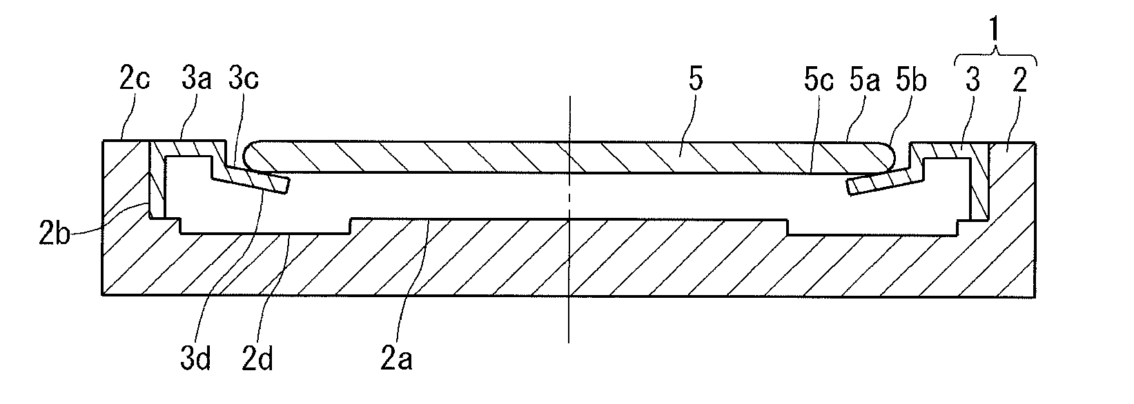
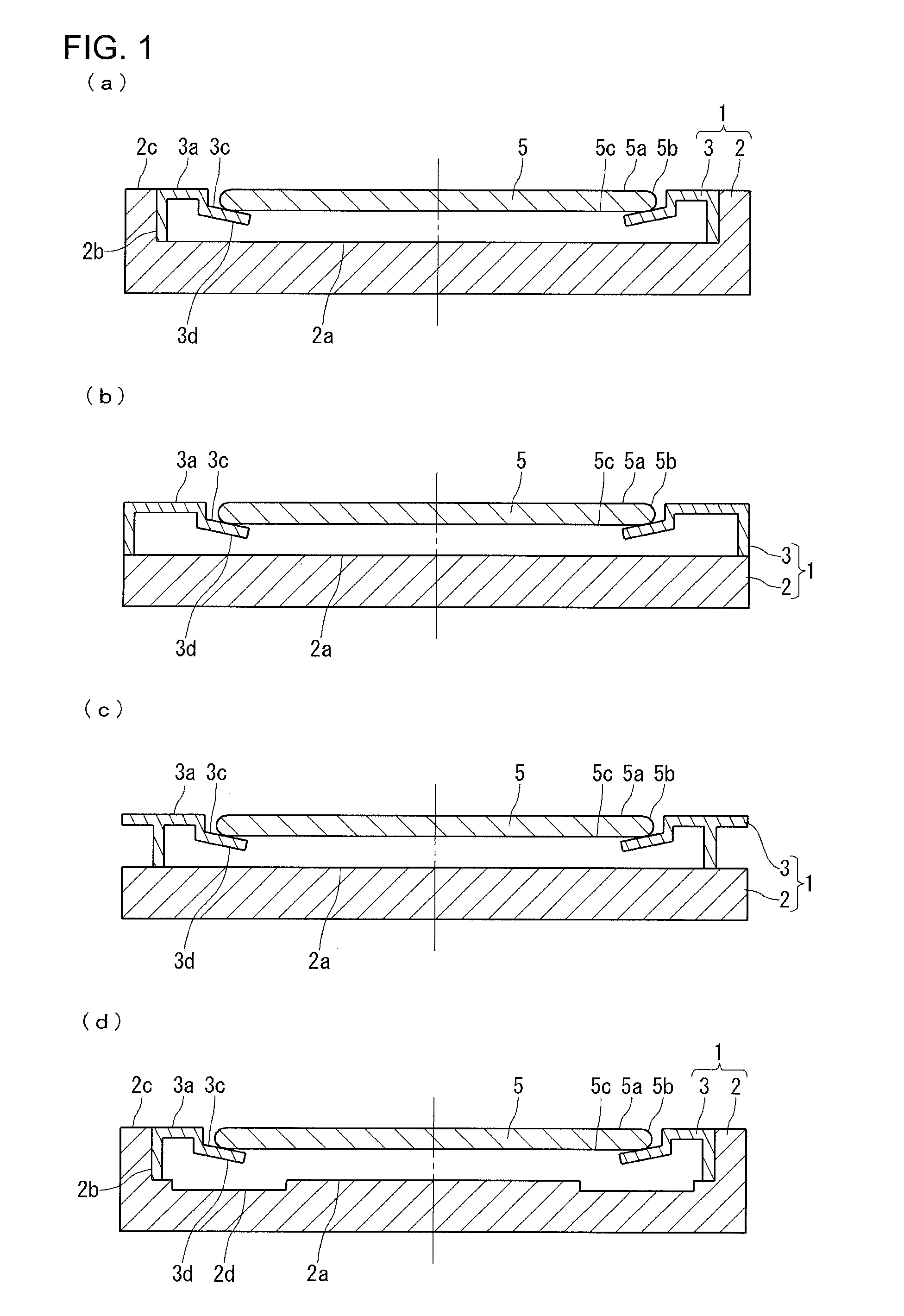
[0048]FIG. 1 are views showing embodiments of the present invention comprising a tray main body and a supporting member, wherein FIG. 1(a), FIG. 1(b), FIG. 1(c) and FIG. 1(d) respectively show one case that a tray main body has a receiving part, another case that a planar tray main body is used and a supporting member is proped in its periphery region, yet another case that a planar tray main body is used and a supporting member is proped around its middle part, and the other case that a concave portion is provided in the tray main body surface that is opposed to a silicon wafer. Tray 1 each shown in FIGS. 1 (a) to (d) comprise a tray main body 2 and a supporting member 3, wherein a silicon wafer 5 is supported and placed on a holding portion 3c disposed in the supporting member 3.

[0049]The tray for CVD of the first embodiment of the present invention is a tray 1, which is used in film forming by a CVD method, comprises a tray main body 2, and a ...

second embodiment

[Tray for CVD as of Second Embodiment]

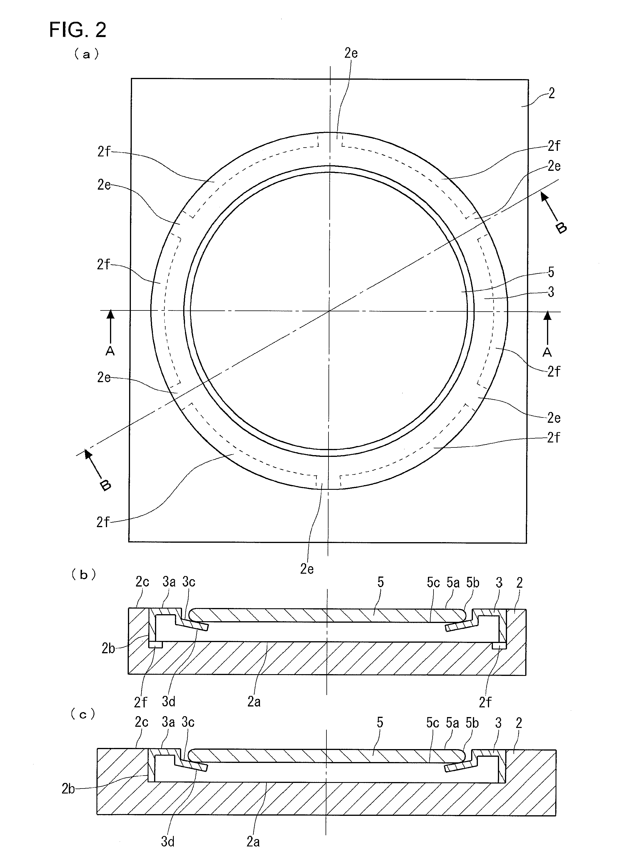
[0058]FIG. 2 are views showing an embodiment of the present invention in which a tray main body is provided with land portions, wherein FIG. 2(a) is a top view, FIG. 2(b) is an A-A cross section in the FIG. 2(a), and FIG. 2(c) is a B-B cross section in the FIG. 2(a). The tray each shown in FIG. 2 comprises a tray main body 2, and a supporting member 3 mounted on the tray main body 2 and supporting a silicon wafer 5. In addition, the supporting member 3 is provided with a holding portion 3c on which the silicon wafer 5 is directly placed, having its lower surface 3d which is apart from the tray main body 2.

[0059]The tray for CVD of the second embodiment of the present invention is characterized in that the tray main body 2 is provided with land portions 2e, and the tray has a structure in which the supporting member 3 is mounted on the land portions 2e, as the structure for reducing the contact area between the supporting member 3 and the tray ma...

third embodiment

[Tray for CVD as of Third Embodiment]

[0066]FIG. 4 are views showing an embodiment of the present invention in which a supporting member is mounted maintaining point contact and line contact, wherein FIG. 4(a) is a top view and FIG. 4(b) is an A-A cross section in the FIG. 4(a). The tray shown in FIG. 4 comprises a tray main body 2 having a concave receiving part for housing a supporting member 3, and the supporting member 3 mounted on the tray main body 2 and supporting a silicon wafer 5. In addition, the supporting member 3 is provided with a holding portion 3c, on which the silicon wafer 5 is directly placed, and also has its lower surface 3d, which is apart from the tray main body 2.

[0067]The tray for CVD of the third embodiment of the present invention is characterized in that the tray has a structure in which the supporting member 3 is mounted on the tray main body 2 maintaining point contact or line contact, as the structure for reducing the contact area between the supporting...


PUM

PropertyMeasurementUnit
Areaaaaaaaaaaa
Distributionaaaaaaaaaa

Abstract

A tray for film formation by a CVD method includes a tray main body (2) and a supporting member (3) mounted on the tray main body (2) for supporting a silicon wafer (5). The supporting member (3) has a holding portion (3c), on which the silicon wafer (5) is directly placed. The holding portion (3c) has its lower surface (3d) apart from a surface (2a) of the tray main body that is opposed to and apart from the supported silicon wafer (5), whereby the thickness distribution of an oxide film formed on the silicon wafer can be made uniform. The tray has a structure for reducing a contact area between the supporting member (3) and the tray main body (2), with the holding portion (3c) having a tilted surface with its inner circumferential side closer to the tray main body surface (2a) that is opposed to the silicon wafer.

Description

TECHNICAL FIELD[0001]The present invention relates to a tray for CVD on which a silicon wafer is placed, which is used in film forming by a CVD method, and a film forming method using the same, and more specifically, a tray for CVD that permits the thickness distribution of an oxide film formed on a surface of the silicon wafer to be uniform, and a film forming method using the same.BACKGROUND ART[0002]In a device process and an epitaxial silicon wafer production process, a protective film and an insulating film are formed on a silicon wafer. For example, in the device process, an oxide film and the like are formed as an interlayer insulating film on the surface side of the silicon wafer to be used as a device fabrication region, then wiring formation and the like are performed.[0003]In addition, in the production process of an epitaxial wafer, when a silicon epitaxial layer with high resistivity is vapor-deposited on a main surface of a silicon single-crystal substrate with low res...

Claims


Application Information

Patent Timeline
IPC IPC(8): C23C16/458H01L21/285
CPCC23C16/4585C23C16/458H01L21/0262
Inventor NAKAYAMA, TAKASHIKABASAWA, TOMOYUKIKIHARA, TAKAYUKI
Owner SUMCO CORP
Why Eureka
Try Eureka