Bonding apparatus and bonding method

a technology of bonding apparatus and bonding method, which is applied in the direction of electrical apparatus, chemistry apparatus and processes, and semiconductor devices, etc., can solve problems such as poor connection, and achieve the effects of reducing the thermal capacity of the substrate, improving the reliability of the bonding constructional members of the work, and improving the bonding constructional members

Inactive Publication Date: 2012-10-04
APIC YAMADA CORP
View PDF6 Cites 55 Cited by
  • Summary
  • Abstract
  • Description
  • Claims
  • Application Information

AI Technical Summary

Benefits of technology

[0022]By employing the bonding apparatus of the present invention, reliability of bonding constructional members of the work, which are adhered by the adhesive, can be improved.
[0023]For example, the semiconductor devices and the substrate are preheated, and then heated to bond the semiconductor device to the substrate at a time, so that occurrence position gaps between the bumps and the terminal sections can be prevented.
[0024]The substrate, on which the semiconductor devices are adhered, is supported, by the supporting means, and separated from the clamping face, so that a thermal capacity of the substrate can be reduced and the substrate, etc. can be heated in a short time. Therefore, poor connection, which is caused by rapidly curing the non-conductive adhesive, can be prevented.
[0025]Further, the heating / pressing step is performed in the reduced-pressure atmosphere or the pressurized atmosphere according to properties of the adhesive. Therefore, influences of voids formed in the adhesive can be restrained, and enough adhesive force for retaining the semiconductor devices can be maintained.

Problems solved by technology

In case of using some types of solder, the adhesive 52 cures before the solder bumps 54 are electrically bonded, so there is a possibility of occurring poor connection.

Method used


Image

  • Bonding apparatus and bonding method
  • Bonding apparatus and bonding method
  • Bonding apparatus and bonding method

Examples


embodiment 1

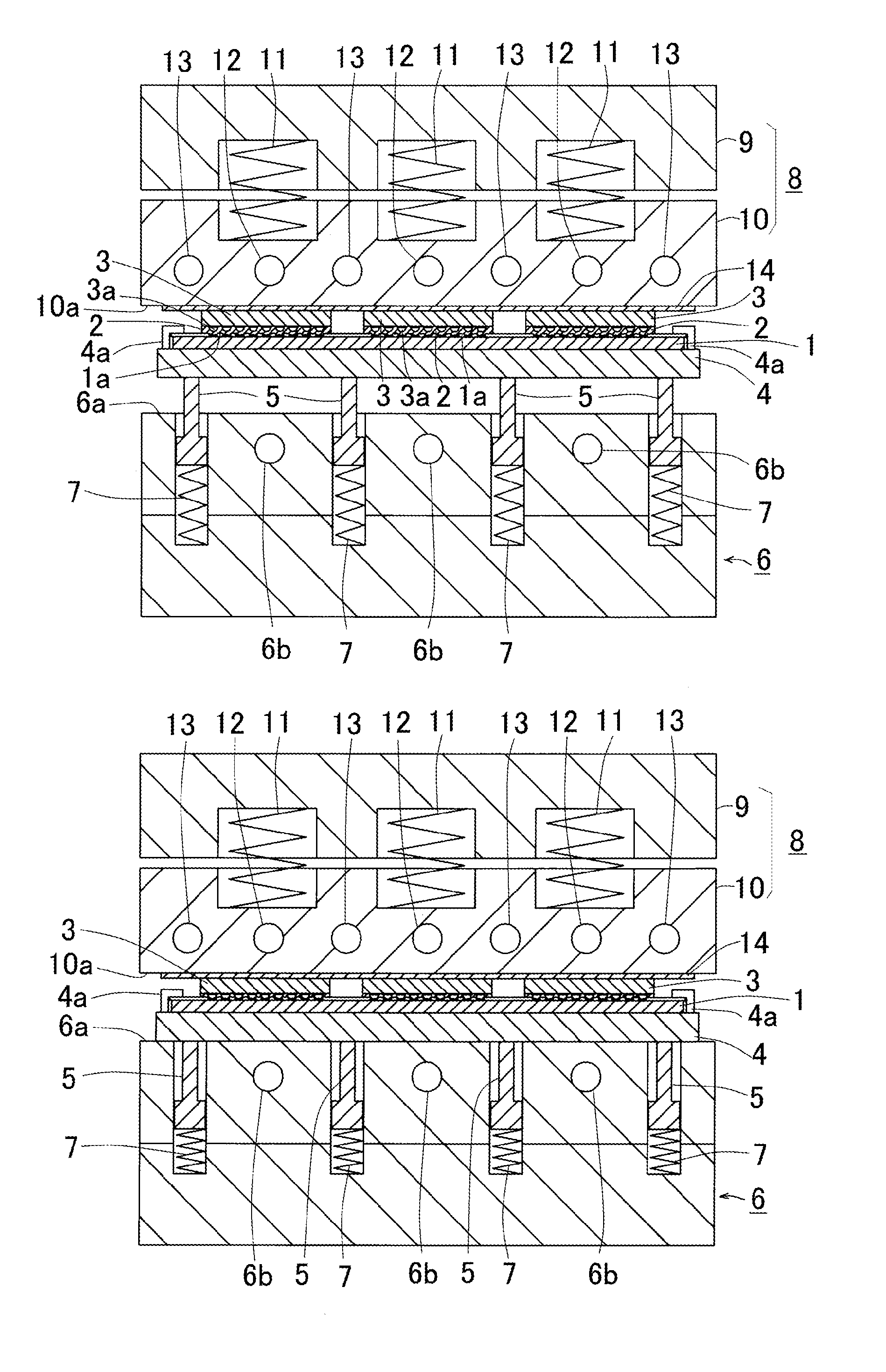
[0051]Embodiment 1 of the present invention will be explained with reference to FIGS. 1A-2B.

[0052]In FIG. 1A, a substrate 1, on which cable patterns have been formed, has terminal sections 1a, on which semiconductor devices 3, e.g., semiconductor chips, are adhered by a thermosetting non-conductive adhesive 2, e.g., NCF, NCP. The substrate 1, on which the semiconductor devices 3 are adhered, is an organic substrate, but other types of substrates, e.g., inorganic ceramic substrate, may be employed. Further, lead frames, semiconductor wafer, etc. may be employed as the substrate. A plurality of lines and rows of the semiconductor devices 3 are adhered by a known flip-chip bonder (not shown).

[0053]Edges of the substrate 1 are held by chucks 4a, so that the substrate 1 is held by a substrate holding plate 4. A bottom face of the substrate holding plate 4 is supported by a plurality of supporting rods 5 so as to hold the substrate 1 without deformation. As shown in FIG. 1A, the supportin...

embodiment 2

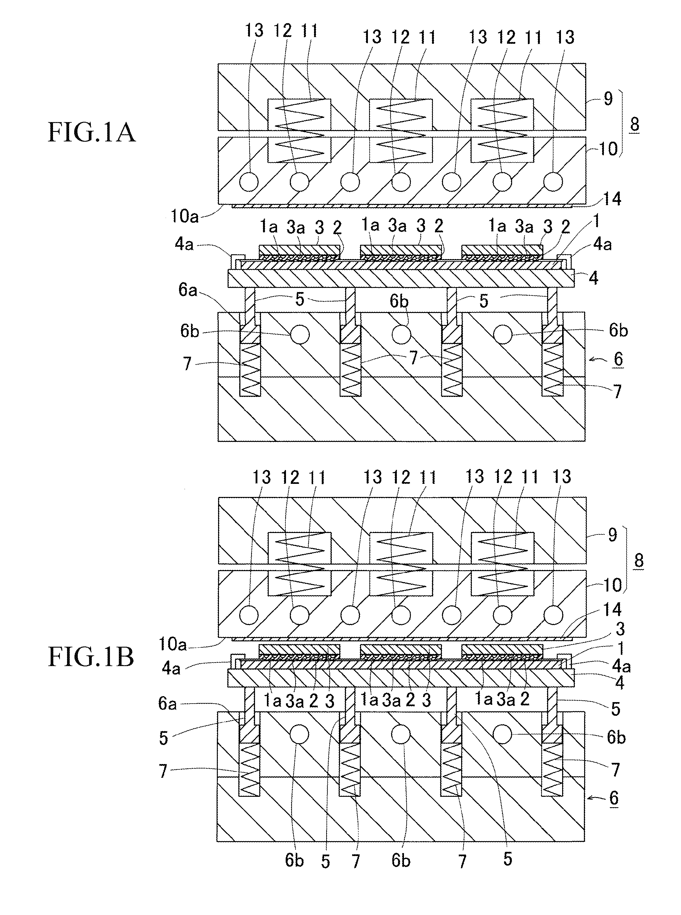
[0071]Next, the apparatus and the method of Embodiment 2 will be explained.

[0072]In comparison with Embodiment 1, the substrate holding plate 4 of the present embodiment has a different structure, and the semiconductor devices 3 are located on the lower side of the substrate 1. Other structural elements of the apparatus of Embodiment 2 are the same as those of Embodiment 1. Therefore, the structural elements described in Embodiment 1 are assigned the same symbols and explanation will be omitted. In the following description, unique structures of Embodiment 2 will be mainly explained.

[0073]In FIG. 4A, supporting sections 4b, whose planar size is slightly smaller than that of the semiconductor devices 3, are upwardly projected from the substrate holding plate 4. Therefore, in the substrate holding plate 4, grooves 4c are formed between the adjacent supporting sections 4b. Edges of the semiconductor devices 3 are not held by the supporting sections 4b, but widths of the edges are small...

embodiment 3

[0081]Next, the apparatus and the method of Embodiment 3 will be explained with reference to FIGS. 6A-7B. Note that, the structural elements described in the above described embodiments are assigned the same symbols and explanation will be omitted.

[0082]In the present embodiment, the substrate 1 is accommodated in a closed space, which is closed by heating / pressing means and supporting means, a reduced-pressure atmosphere or a pressurized atmosphere is produced in the closed space, and then the semiconductor devices 3 are heated and pressed in the closed space.

[0083]As shown in FIG. 6A, a substrate holding plate 15 has an air path 15a and a plurality of sucking holes 15b, which are opened in a surface. An air tube 16a of a sucking mechanism 16, which is provided in a lower die block 19, is connected to the air path 15a. A stretchy spiral tube 16b is provided to a part of the air tube 16a. When the substrate holding plate 15 is pressed by the upper die 8, the spiral tube 16b absorbs ...


PUM

PropertyMeasurementUnit
temperatureaaaaaaaaaa
melting pointaaaaaaaaaa

Abstract

The bonding apparatus is capable of effectively increasing temperature of a substrate and reducing occurrence of position gaps and poor connection in a process of flip-chip-bonding semiconductor devices to the substrate. The bonding apparatus comprises: a supporting unit for supporting the substrate, on which the semiconductor devices have been adhered by a non-conductive; and a heating/pressing unit for heating and pressing the substrate, the heating/pressing unit having a built-in heat source and a clamping face, onto which the substrate supported by the supporting unit is pressed. The substrate supported by the supporting unit is moved toward the clamping face of the heating/pressing unit so as to preheat the substrate and the semiconductor devices by radiation heat. Then, the semiconductor devices are pressed onto the clamping face of the heating/pressing unit so as to cure the non-conductive adhesive and bond bumps of the semiconductor devices to terminal sections of the substrate.

Description

CROSS-REFERENCE TO RELATED APPLICATION[0001]This application is based upon and claims the benefit of priority of the prior Japanese Patent Applications No. P2010-020978 (filed on Feb. 2, 2010), P2011-069344 (filed on Mar. 28, 2011) and P2011-099610 (filed on Apr. 27, 2011) and the entire contents of which are incorporated herein by reference.FIELD[0002]The present invention relates to a bonding apparatus and a bonding method for, for example, flip-chip-bonding bumps of semiconductor devices, which are adhered on a substrate by a non-conductive adhesive, to terminal sections of the substrate.BACKGROUND[0003]In FIG. 23A, cable patterns are formed on a substrate 51, and semiconductor devices (flip chips) 53 are adhered to terminal sections 51a of the substrate 51 by applying a non-conductive adhesive 52, e.g., NCF (non-conductive film), NCP (non-conductive paste). In this state, metal bumps 54, e.g., solder bumps, gold bumps, of the semiconductor devices 53 are not electrically bonded ...

Claims


Application Information

Patent Timeline
Patent Type & Authority Applications(United States)
IPC IPC(8): B29C65/18B32B37/02
CPCH01L24/75H01L24/81H01L2924/07802H01L2224/32225H01L2224/16225H01L2924/014H01L2924/01074H01L24/83H01L24/92H01L24/95H01L2224/73204H01L2224/75102H01L2224/75252H01L2224/753H01L2224/75313H01L2224/75315H01L2224/75317H01L2224/7532H01L2224/755H01L2224/75704H01L2224/75755H01L2224/75756H01L2224/75804H01L2224/7598H01L2224/75984H01L2224/81048H01L2224/8109H01L2224/81093H01L2224/83048H01L2224/8309H01L2224/83093H01L2224/83855H01L2224/9211H01L2224/95093H01L2224/97H01L2924/01029H01L2924/01033H01L2924/01079H01L2924/01082H01L2924/09701H01L2924/01005H01L2924/01006H01L2924/01019H01L2924/00H01L2224/75502H01L2924/15787
Inventor KOBAYASHI, KAZUHIKO
Owner APIC YAMADA CORP
Why Eureka
Try Eureka