

Plasma processing apparatus and plasma processing method
a plasma processing apparatus and plasma technology, applied in the field of plasma processing apparatus, can solve the problem that no reactance device may be connected to the inner coil, and achieve the effect of effective and easy control of plasma density distribution, low plasma density, and expansion of the freedom degree of plasma density distribution control on the substra
- Summary
- Abstract
- Description
- Claims
- Application Information
AI Technical Summary
Benefits of technology
Problems solved by technology
Method used
Image

Examples
Embodiment Construction
[0042]Hereinafter, illustrative embodiments will be described with reference to the accompanying drawings.
[Entire Configuration and Operation of Apparatus]
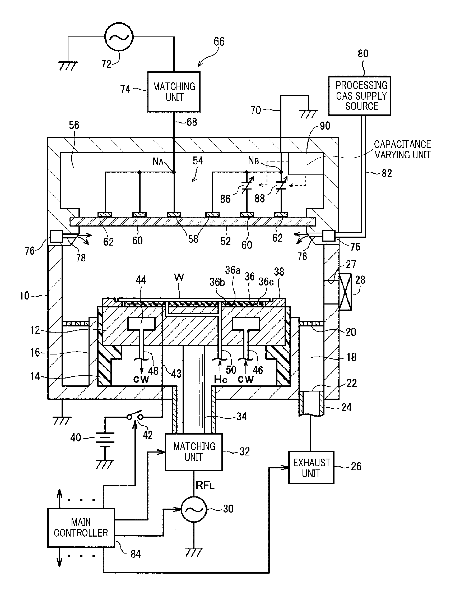
[0043]FIG. 1 illustrates a configuration of an inductively coupled plasma processing apparatus in accordance with an illustrative embodiment.
[0044]The plasma processing apparatus is configured as an inductively coupled plasma etching apparatus using a planar coil RF antenna. By way of example, the plasma etching apparatus may include a cylindrical vacuum chamber (processing chamber) 10 made of metal such as aluminum or stainless steel. The chamber 10 may be frame grounded.
[0045]Above all, there will be explained a configuration of each component which is not related to plasma generation in this inductively coupled plasma etching apparatus.
[0046]At a lower central region within the chamber 10, a circular plate-shaped susceptor 12 may be provided horizontally. The susceptor 12 may mount thereon a target substrate such as a semicondu...
PUM
| Property | Measurement | Unit |
|---|---|---|
| frequency | aaaaa | aaaaa |
| impedances | aaaaa | aaaaa |
| impedances | aaaaa | aaaaa |
Abstract
Description
Claims
Application Information