Semiconductor device and method of manufacturing the same
a semiconductor and device technology, applied in semiconductor devices, semiconductor/solid-state device details, electrical apparatus, etc., can solve the problems of reducing so as to reduce the reliability of connection of bumps and reduce the viscosity of polymers. , the effect of low heat resistan
- Summary
- Abstract
- Description
- Claims
- Application Information
AI Technical Summary
Benefits of technology
Problems solved by technology
Method used
Image
Examples
first embodiment
[0051]A semiconductor device according the present embodiment is a layered-type semiconductor device obtained by bonding two silicon wafers on whose main surfaces a plurality of bump electrodes and a polymer film for surrounding their peripheries are formed, and electrically connecting integrated circuits to each other formed on the respective silicon wafers via a bump electrode.
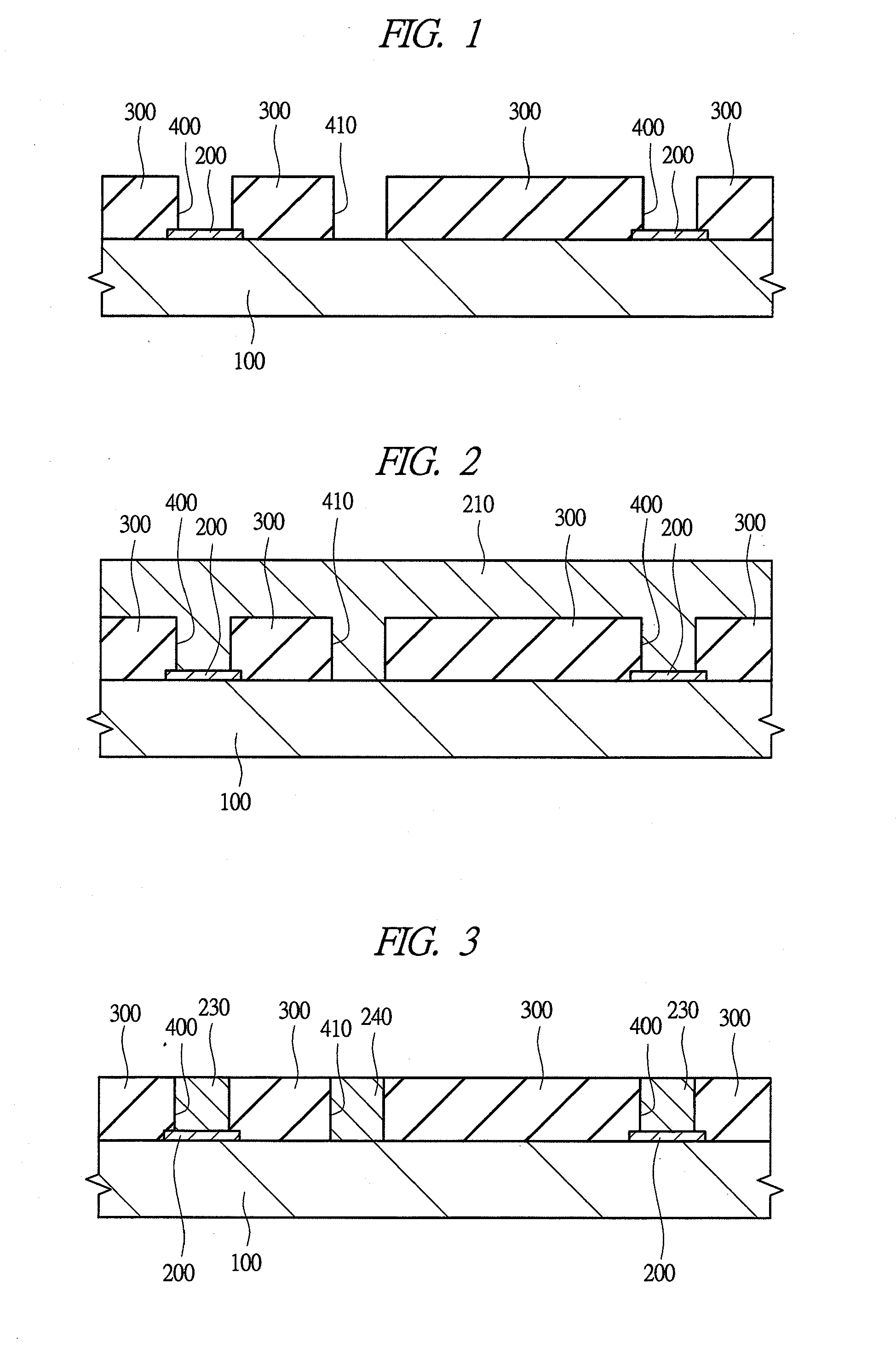
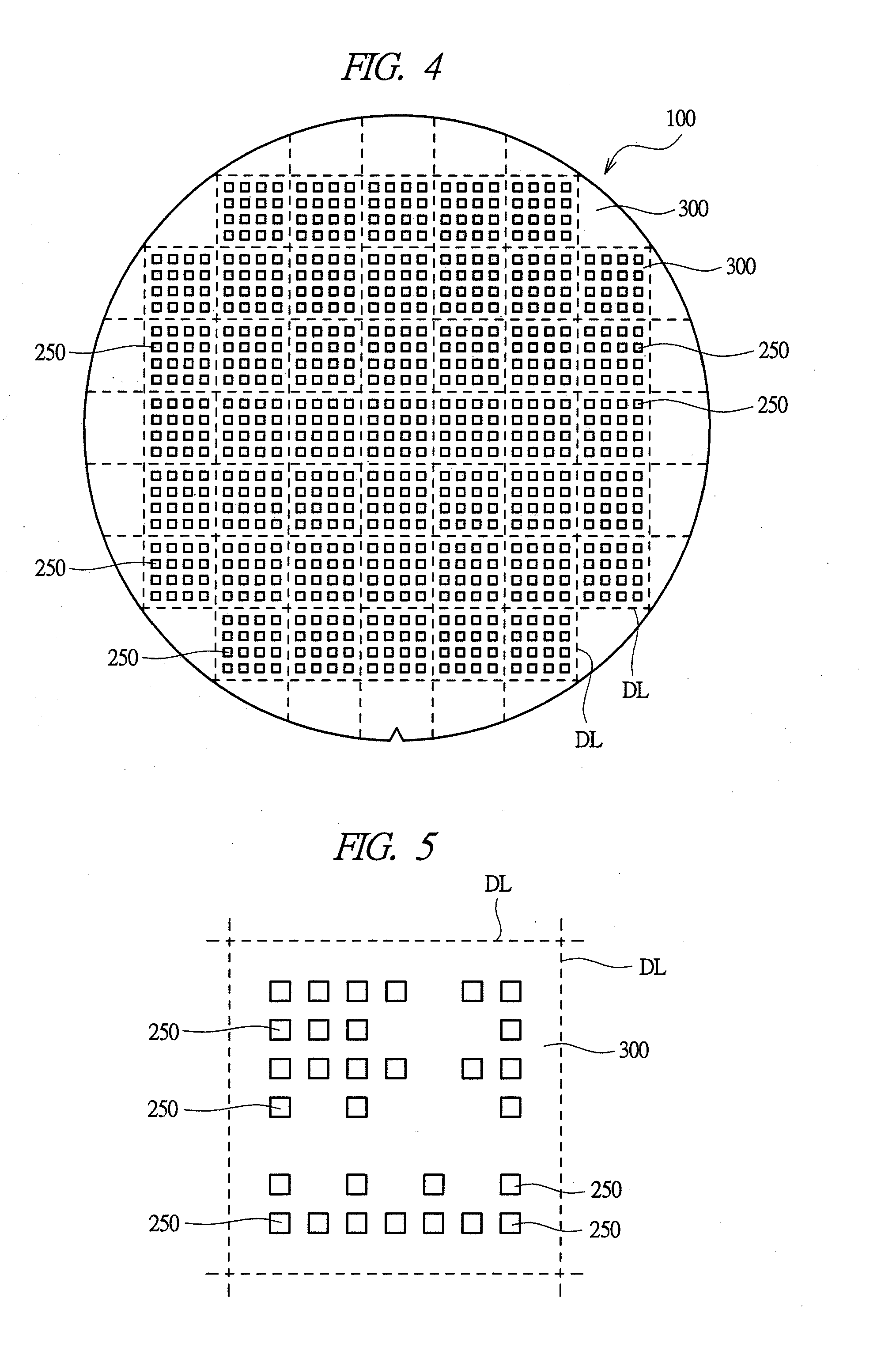
[0052]Hereinafter, with reference to FIGS. 1 to 9, a method of manufacturing the semiconductor device of the present embodiment will be explained in an order of steps. FIGS. 1 to 3, 7 and 8 are cross-sectional views of principal parts each explaining a manufacturing step for a layered semiconductor according to the first embodiment of the present invention, FIGS. 4 to 6 are planar layouts illustrating arrangement of the bump of the layered semiconductor during the manufacturing step, and FIG. 9 is a planar layout illustrating a modification example of the semiconductor device of the present embodiment.
[0053]...
second embodiment
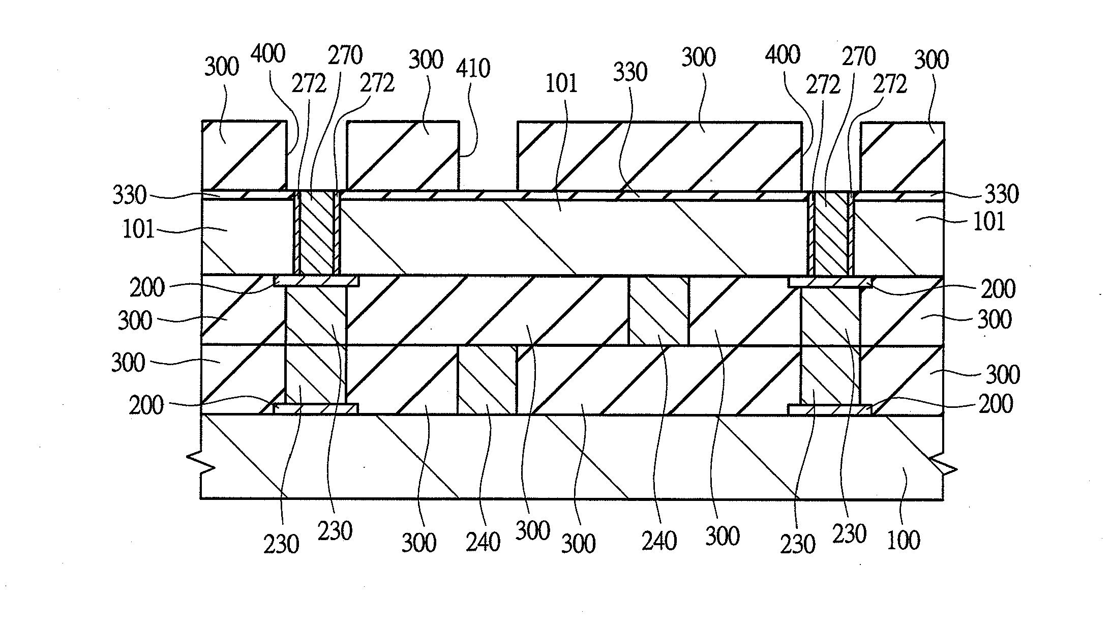
[0127]In a present embodiment, an example of a semiconductor device obtained by bonding a front surface of a silicon substrate on which a semiconductor element is formed and a rear surface on which the semiconductor element is not formed to each other will be explained with reference to FIGS. 11 to 14. Note that the explanation of a configuration with the same reference symbols and portions having the same functions as those of the configuration described above in the first embodiment will be omitted. FIGS. 11 to 14 are cross-sectional views of principal parts each explaining a manufacturing process of a layered semiconductor of the present embodiment.
[0128]First, as illustrated in FIG. 11, a rear-surface insulating film 330 formed of, for example, a silicon oxide film is formed on a rear surface of a first silicon substrate 100 on which a semiconductor element is not formed, and then, a through electrode 270 for electrical connection to a main surface of the first silicon substrate...
PUM
| Property | Measurement | Unit |
|---|---|---|
| melting point | aaaaa | aaaaa |
| temperature | aaaaa | aaaaa |
| melting point | aaaaa | aaaaa |
Abstract
Description
Claims
Application Information


