RC-triggered Semiconductor Controlled Rectifier for ESD Protection of Signal Pads

a technology of esd protection and semiconductor control, applied in emergency protective circuit arrangements, instruments, etc., can solve problems such as reducing device dimensions, large damage to the integrated circuit, and large currents

Active Publication Date: 2012-10-11
IBM CORP
View PDF4 Cites 44 Cited by
  • Summary
  • Abstract
  • Description
  • Claims
  • Application Information

AI Technical Summary

Benefits of technology

[0007]In another embodiment, a method is provided for fabricating an integrated circuit with protection from an ESD event. The method includes connecting a signal pad to an SCR and connecting the SCR to a trigger circuit configured to maintain the SCR in a high impedance state in the absence of an ESD event and to trigger the SCR into a low impedance

Problems solved by technology

Chips may be exposed to electrostatic discharge (ESD) events leading to potentially large and damaging currents within the integ

Method used


Image

  • RC-triggered Semiconductor Controlled Rectifier for ESD Protection of Signal Pads
  • RC-triggered Semiconductor Controlled Rectifier for ESD Protection of Signal Pads
  • RC-triggered Semiconductor Controlled Rectifier for ESD Protection of Signal Pads

Examples


Embodiment Construction

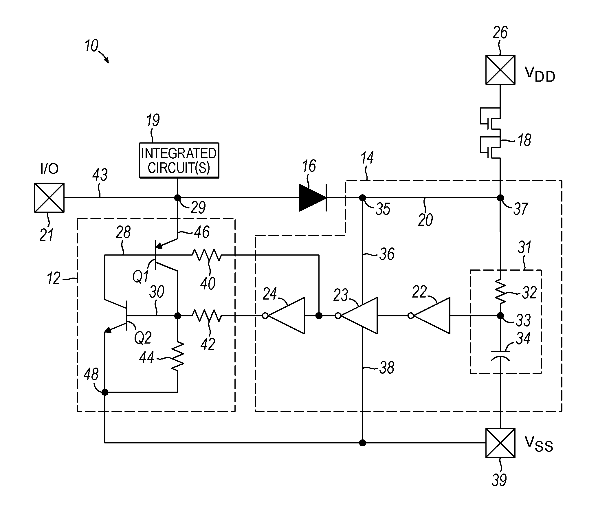
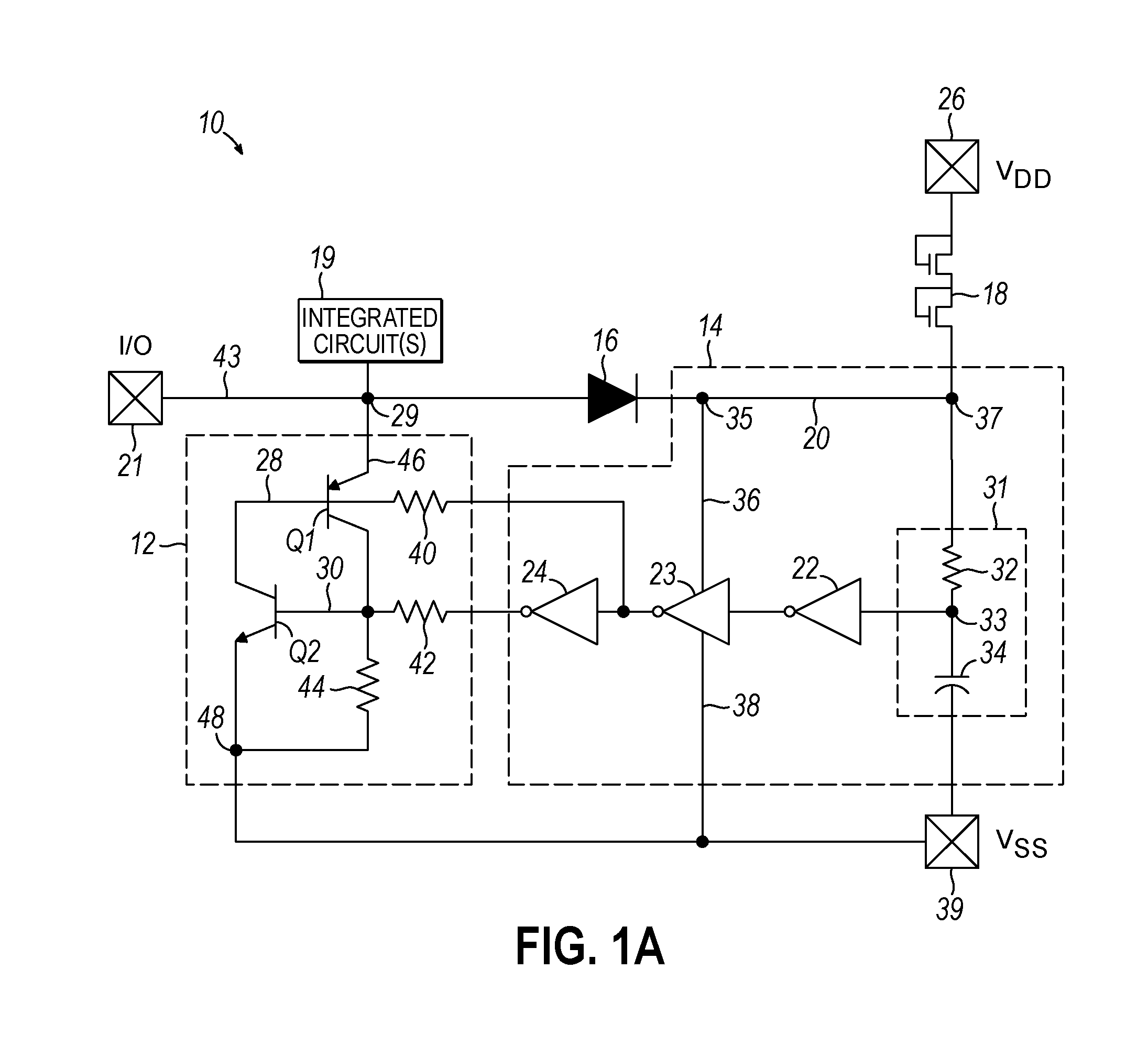
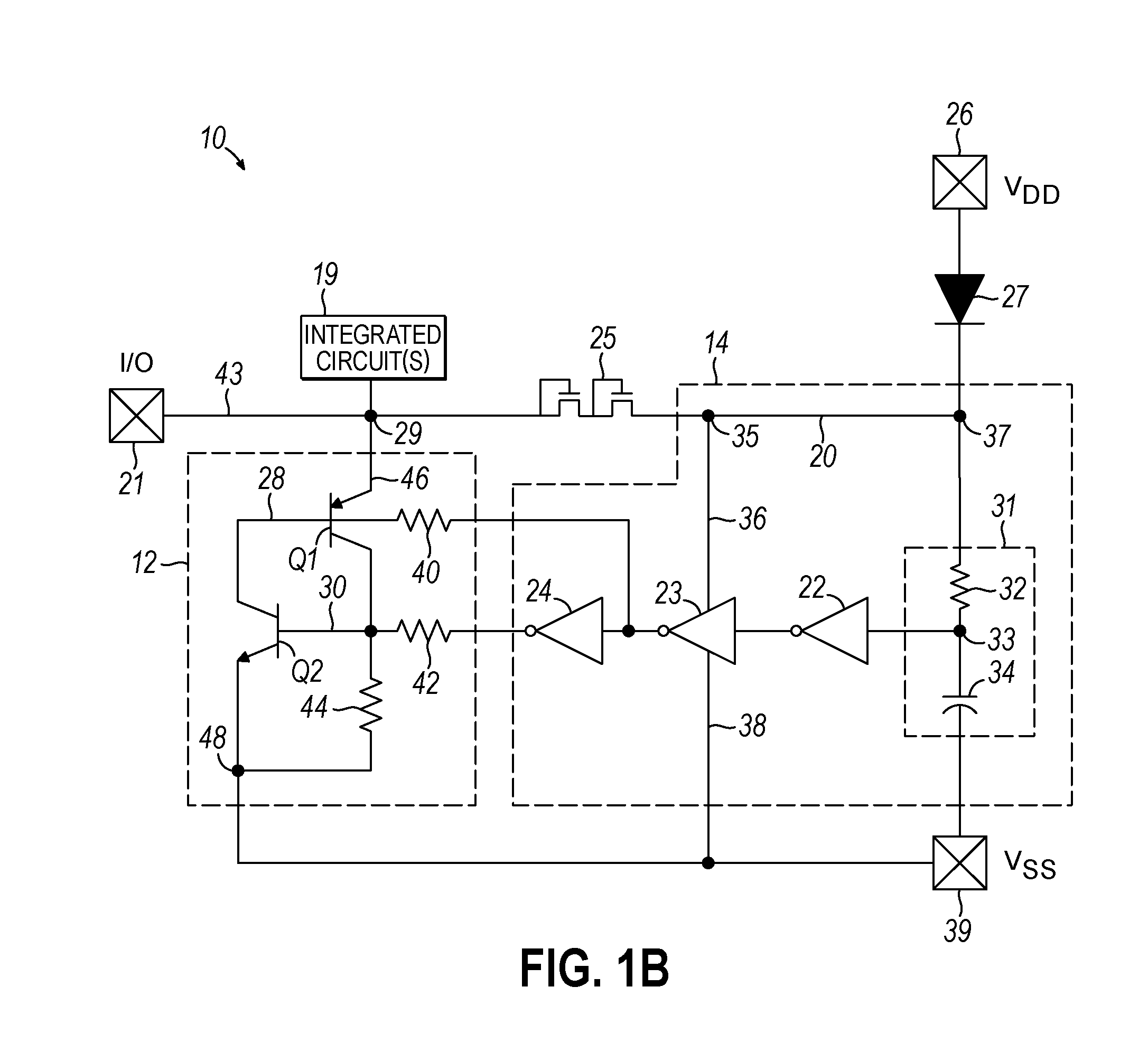
[0018]Embodiments of the invention are related to an ESD protection circuit for an input / output (I / O) signal pad of an integrated circuit, or chip. The ESD protection circuit includes a semiconductor controlled rectifier (SCR) and an RC-trigger circuit coupled to the signal pad by an isolation diode. During normal operation, the isolation diode is reverse biased, so that the RC-trigger circuit is electrically isolated from the signal pad. When the chip is unpowered (whether the chip is loose or is installed (e.g., surface mounted) on a printed circuit board), an electro-static discharge (ESD) event may forward bias the isolation diode, thereby causing the RC-trigger circuit to trigger the SCR so that the ESD current is shunted away from the signal pad to a chip voltage supply rail. The ESD protection is provided with reduced capacitive loading of the protected signal pad. An additional diode, which may implemented as a diode-connected transistor string, may couple the RC-trigger cir...


PUM

PropertyMeasurementUnit
Electric potential / voltageaaaaaaaaaa
Electrical impedanceaaaaaaaaaa
Electric impedanceaaaaaaaaaa

Abstract

RC-trigger circuits for a semiconductor controlled rectifier (SCR), methods of providing electrostatic discharge (ESD) protection, and design structures for a RC-trigger circuit. The RC-trigger circuit is coupled to an input/output (I/O) signal pad by an isolation diode and is coupled to a power supply voltage by a power supply diode. Under normal operating conditions, the isolation diode is reverse biased, isolating the RC-trigger circuit from the input/output (I/O) pad, and the power supply diode is forward biased so that the RC-trigger circuit is supplied with power. The isolation diode may become forward biased during ESD events while the chip is unpowered, causing the RC-trigger circuit to trigger an SCR configured protect the signal pad from ESD into a conductive state. The power supply diode may become reverse biased during the ESD event, which isolates the power supply rail from the ESD voltage pulse.

Description

BACKGROUND[0001]The present invention relates generally to semiconductor device fabrication and, more particularly, to electrostatic discharge (ESD) circuits for protecting an Input / Output (I / O) signal pad in radio frequency and other high frequency signal applications, as well as methods for providing ESD protection and design structures for an ESD protection circuit.[0002]Modern electronics achieve high levels of functionality in small form factors by integrating multiple functions onto a single chip. A common fabrication process that allows high levels of integration at a relatively low cost is Complementary Metal-Oxide-Semiconductor (CMOS). CMOS processes build a combination of p-type and n-type metal-oxide-semiconductor field-effect transistors (MOSFETs) to implement logic gates and other types of digital circuits.[0003]Chips may be exposed to electrostatic discharge (ESD) events leading to potentially large and damaging currents within the integrated circuit. Increasing integr...

Claims


Application Information

Patent Timeline
IPC IPC(8): H02H9/04H05K13/00G06F17/50
CPCH01L27/0262Y10T29/49002H03K19/00361H02H9/046
Inventor ABOU-KHALIL, MICHEL J.GAUTHIER, JR., ROBERT J.LEE, TOM C.LI, JUNJUNMITRA, SOUVICKPUTNAM, CHRISTOPHER S.
Owner IBM CORP
Why Eureka
Try Eureka