Phosphor reflecting sheet, light emitting diode device, and producing method thereof

a technology of light-emitting diodes and reflecting sheets, which is applied in the direction of optics, instruments, optical elements, etc., can solve the problems and achieve the effect of reducing the light extraction efficiency

Inactive Publication Date: 2012-10-18
NITTO DENKO CORP
View PDF12 Cites 41 Cited by
  • Summary
  • Abstract
  • Description
  • Claims
  • Application Information

AI Technical Summary

Benefits of technology

[0011]However, in the white light emitting device obtained by the producing method in Japanese Unexamined Patent Publication No. 2005-191420, there is a disadvantage that the semiconductor light emitting element is spaced apart from the reflecting frame portion, so that a part of the light emitted from the semiconductor light emitting element toward the side is absorbed in the encapsulating portion before being reflected at the reflecting frame portion and as a result, extraction efficiency of the light is reduced.

Problems solved by technology

However, in the white light emitting device obtained by the producing method in Japanese Unexamined Patent Publication No. 2005-191420, there is a disadvantage that the semiconductor light emitting element is spaced apart from the reflecting frame portion, so that a part of the light emitted from the semiconductor light emitting element toward the side is absorbed in the encapsulating portion before being reflected at the reflecting frame portion and as a result, extraction efficiency of the light is reduced.

Method used


Image

  • Phosphor reflecting sheet, light emitting diode device, and producing method thereof
  • Phosphor reflecting sheet, light emitting diode device, and producing method thereof
  • Phosphor reflecting sheet, light emitting diode device, and producing method thereof

Examples


example 1

The Embodiments in FIGS. 2 and 3

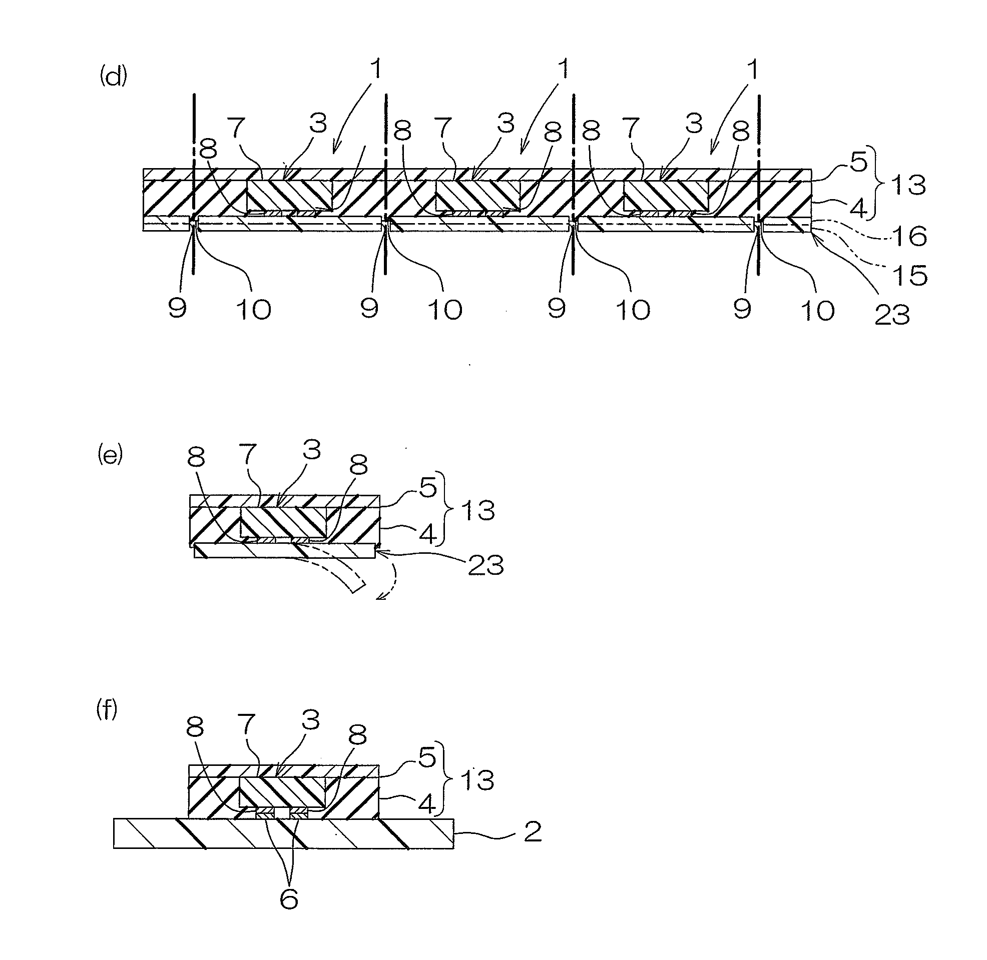
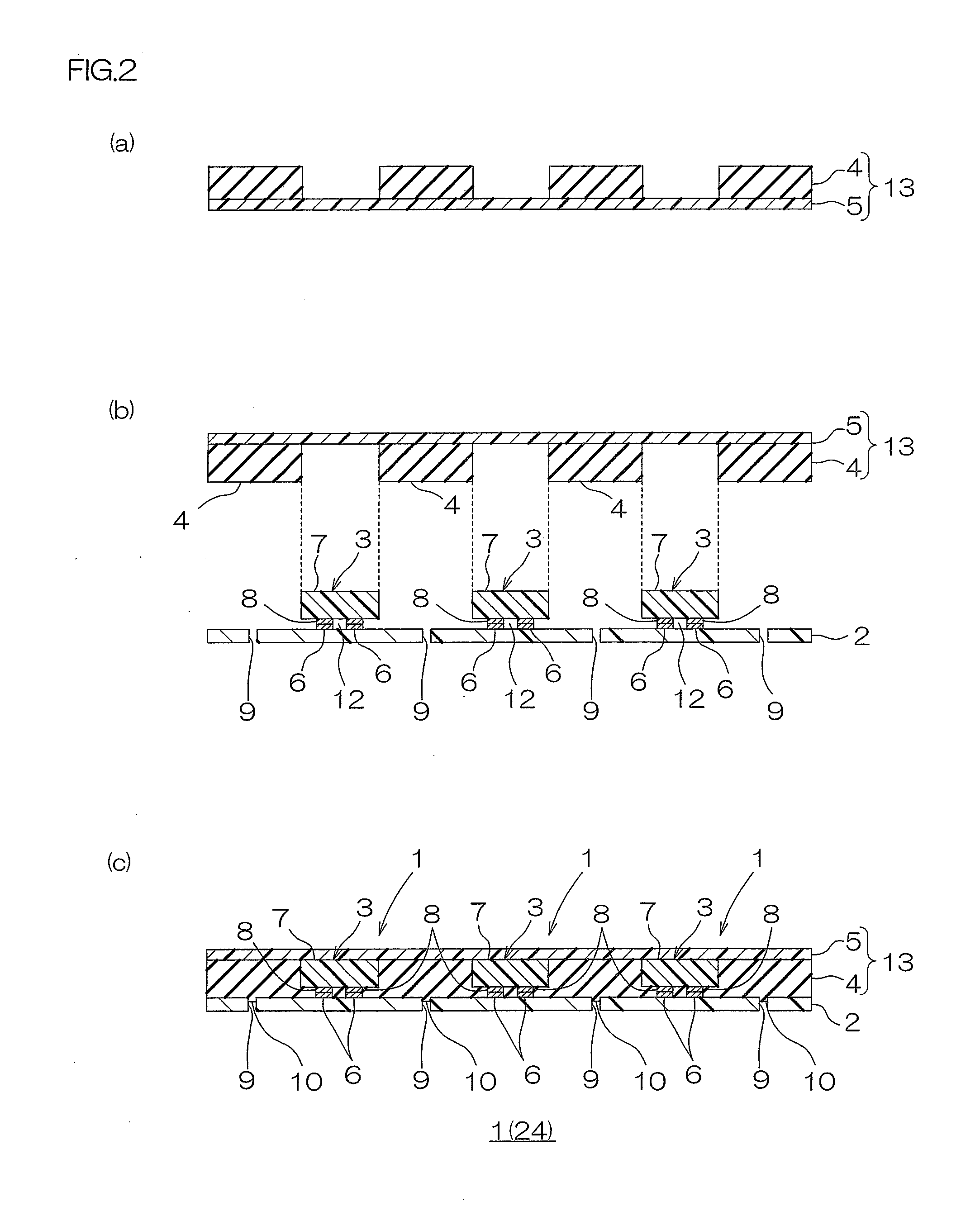
[0206]First, a phosphor reflecting sheet was prepared (ref: FIG. 2(a)).

[0207]That is, a first release substrate made of polyethylene terephthalate having a thickness of 50 μm was first prepared. Then, 26 parts by mass of phosphor particles composed of Y3Al5O12:Ce (in a sphere shape, the average particle size of 8 μm) and 74 parts by mass of a silicone resin (addition reaction type silicone resin, kinetic viscosity (at 25° C.) of 20 mm2 / s, manufactured by WACKER ASAHIKASEI SILICONE CO., LTD.) were blended and stirred uniformly, so that a phosphor composition was prepared. The phosphor composition was applied onto the entire upper surface of the prepared first release substrate to form a phosphor film. Then, the phosphor film was dried at 100° C. to form a phosphor layer on the entire upper surface of the first release substrate (ref: FIG. 4(a)).

[0208]Then, a mask made of stainless steel having a thickness of 100 μm was disposed on the upper surface of ...

example 2

The Embodiments in FIGS. 6 and 7

[0225]A second release substrate formed of a thermal release sheet (a trade name “REVALPHA”, manufactured by NITTO DENKO CORPORATION) having a thickness of 100 μm was prepared (ref: FIG. 6(a)).

[0226]Then, light emitting diode elements each having a thickness of 0.1 mm and including a light semiconductor layer including a buffer layer (GaN); an N-type semiconductor layer (n-GaN); a light emitting layer (InGaN); and a P-type semiconductor layer (p-GaN:Mg) and an electrode portion including an anode electrode and a cathode electrode were provided on the upper surface of the second release substrate (ref: the lower portion in FIG. 6(b)).

[0227]Additionally, through holes each in a circular shape in plane view having an inner diameter of 100 μm were formed in the second release substrate by drilling perforation.

[0228]Subsequently, a phosphor reflecting sheet was prepared (ref: the upper portion in FIG. 6(b)).

[0229]That is, in the same manner as in Example 1...


PUM


Abstract

A phosphor reflecting sheet provides a phosphor layer on one side in a thickness direction of a light emitting diode element and provides a reflecting resin layer at the side of the light emitting diode element. The phosphor reflecting sheet includes the phosphor layer and the reflecting resin layer provided on one surface in the thickness direction of the phosphor layer. The reflecting resin layer is formed corresponding to the light emitting diode element so as to be disposed in opposed relation to the side surface of the light emitting diode element.

Description

CROSS-REFERENCE TO RELATED APPLICATION[0001]The present application claims priority from Japanese Patent Application No. 2011-089955 filed on Apr. 14, 2011, the contents of which are hereby incorporated by reference into this application.BACKGROUND OF THE INVENTION[0002]1. Field of the Invention[0003]The present invention relates to a phosphor reflecting sheet, a light emitting diode device, and a producing method thereof, to be specific, to a producing method of a light emitting diode device, a phosphor reflecting sheet used in the producing method, and a light emitting diode device obtained by the producing method of the light emitting diode device.[0004]2. Description of Related Art[0005]In recent years, as a light emitting device that is capable of emitting high-energy light, a white light emitting device has been known. In the white light emitting device, for example, a diode board; an LED (light emitting diode) laminated thereon, emitting blue light; a phosphor layer that can ...

Claims


Application Information

Patent Timeline
Patent Type & Authority Applications(United States)
IPC IPC(8): H01L33/50G02B5/08H01L33/60
CPCH01L33/46H01L33/505H01L33/56H01L2933/005H01L24/97H01L2924/12041H01L2224/16H01L2924/00H01L2924/12042H01L2924/15787H01L33/50H01L33/60
Inventor OOYABU, YASUNARIITO, HISATAKANISHIOKA, TSUTOMUNAITO, TOSHIKI
Owner NITTO DENKO CORP
Why Eureka
Try Eureka