

Reducing Narrow Gate Width Effects in an Integrated Circuit Design
a technology of integrated circuits and gate widths, applied in the field of transistor sizing, can solve the problems of narrow gate width effects, device difficulty in turning on or operating reliably, and vt becoming too large for a given operating voltage, so as to reduce the narrow gate width effect and the smallest possible area
- Summary
- Abstract
- Description
- Claims
- Application Information
AI Technical Summary
Benefits of technology
Problems solved by technology
Method used
Image

Examples
Embodiment Construction
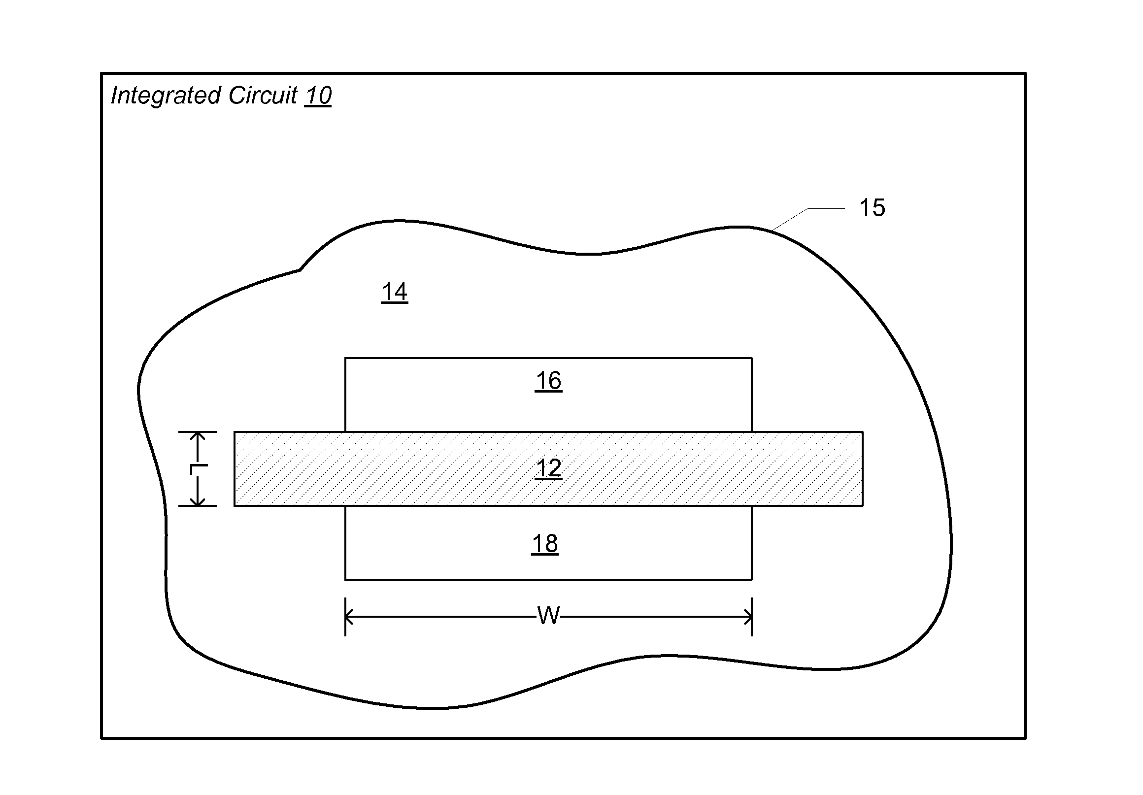
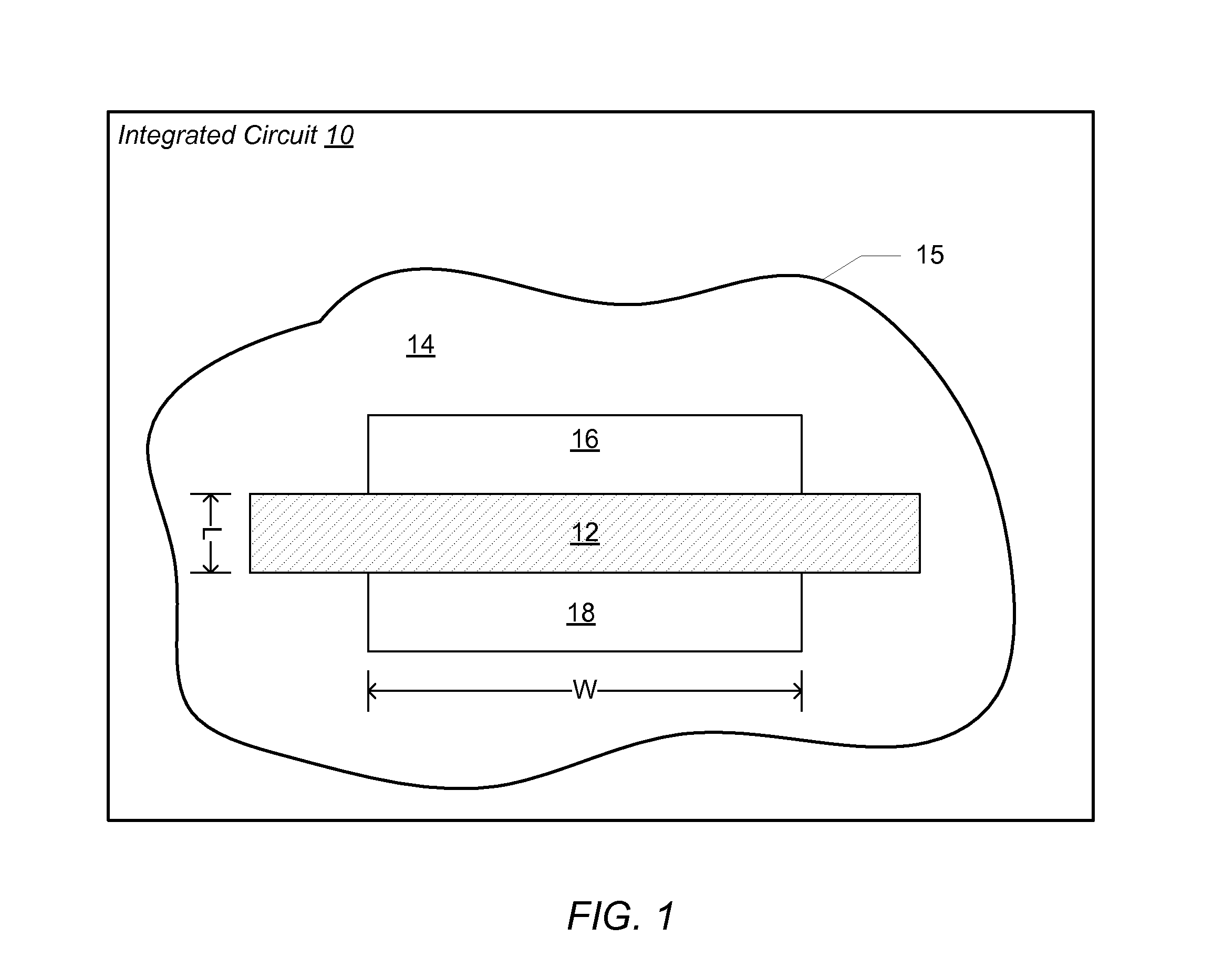
[0006]Various embodiments of a method for reducing narrow gate width effects in an integrated circuit design are disclosed. Broadly speaking, a method is contemplated for finding the smallest possible transistor channel widths for library cells that produce logic blocks that meet timing constraints while using the least amount of power and have the smallest possible area. The smallest channel width that can best meet the design criteria is not always the minimum width for the technology.
[0007]In one embodiment, the method includes creating an integrated circuit device library that includes one or more cells. Each cell may have a number of transistors. Each of the transistors may be specified to have a minimum channel width that may be determined by the manufacturing capability of a particular manufacturing facility within which the integrated circuit may be manufactured. The method may also include characterizing the device library while varying process, voltage and temperature para...
PUM
 Abstract
Description
Claims
Application Information