Supercharge Your Innovation With Domain-Expert AI Agents!

Resurf structure and ldmos device

a technology of resurf structure and ldmos, applied in the direction of semiconductor devices, basic electric elements, electrical apparatus, etc., can solve the problems of 1-dimensional charge balancing, device performance is only enhanced to a limited extent, and achieve the effect of enhancing device performan

Active Publication Date: 2012-11-08
EPISIL TECH
View PDF3 Cites 19 Cited by
  • Summary
  • Abstract
  • Description
  • Claims
  • Application Information

AI Technical Summary

Benefits of technology

[0007]In light of the above, the present invention provides a RESURF structure and an LDMOS device including the structure, so that the position of the P-type doped region is deeper, and 2-dimensional charge balancing is further achieved. Moreover, the concentration in an N-type drifting region is also increased, thereby enhancing device performance.
[0028]In summary, in the structure according to the present invention, at least one trench insulating structure and at least one doped region are disposed in the substrate, and the doped region surrounds the sidewall and the bottom of the trench insulating structure, so as to reduce the surface field. According to the present invention, the trench is first formed and a tilted ion implantation process is then performed, so that the position of the P-type doped region is deeper, and 2-dimensional charge balancing is further achieved. Moreover, the concentration in the N-type drifting region is also increased, thereby enhancing device performance.

Problems solved by technology

The doped region is limited by the implantation energy and can only be formed at the surface, so that only 1-dimensional charge balancing can be achieved, and device performance is only enhanced to a limited extent.

Method used


Image

  • Resurf structure and ldmos device
  • Resurf structure and ldmos device
  • Resurf structure and ldmos device

Examples


Embodiment Construction

[0037]Reference will now be made in detail to the present preferred embodiments of the invention, examples of which are illustrated in the accompanying drawings. Wherever possible, the same reference numbers are used in the drawings and the description to refer to the same or like parts.

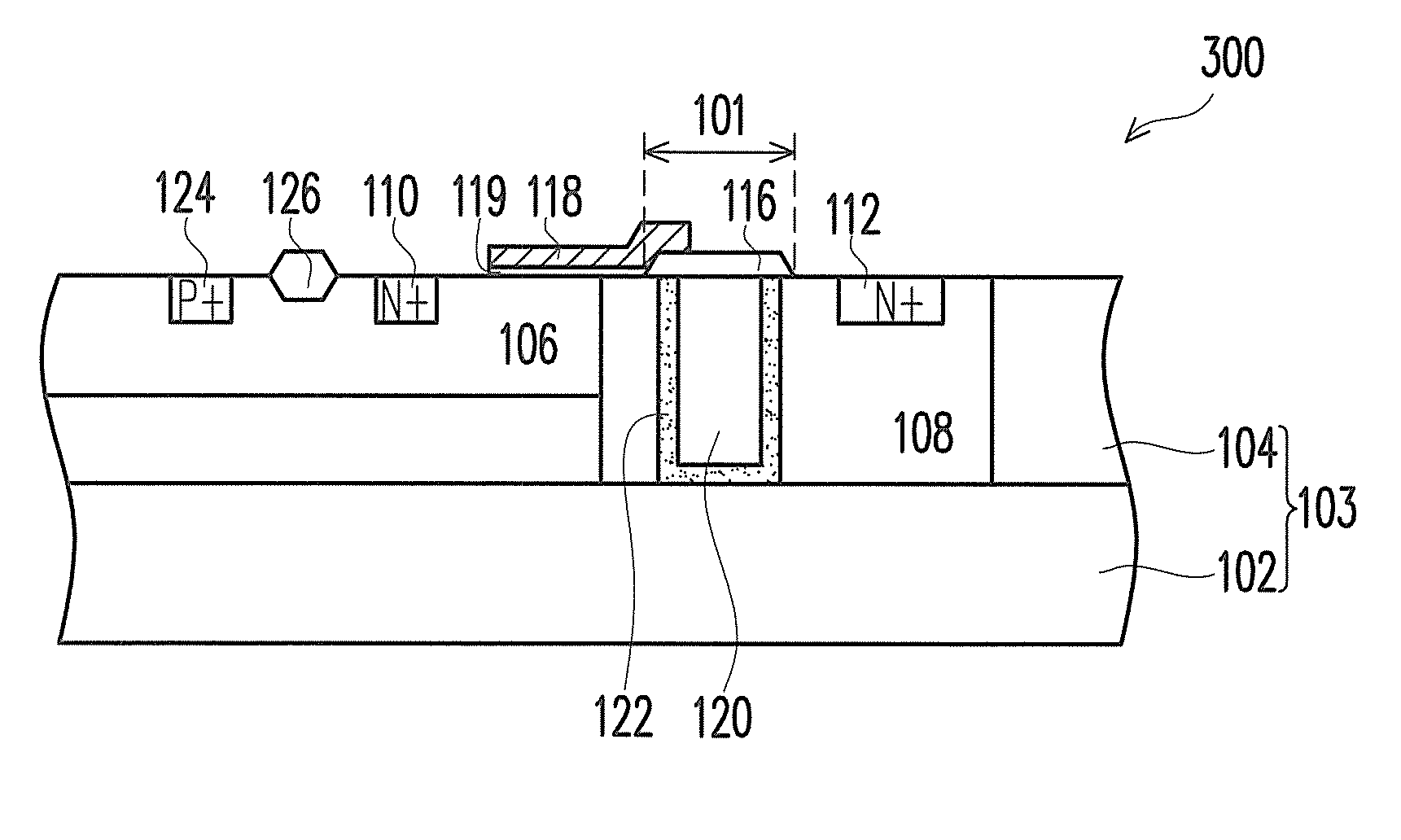
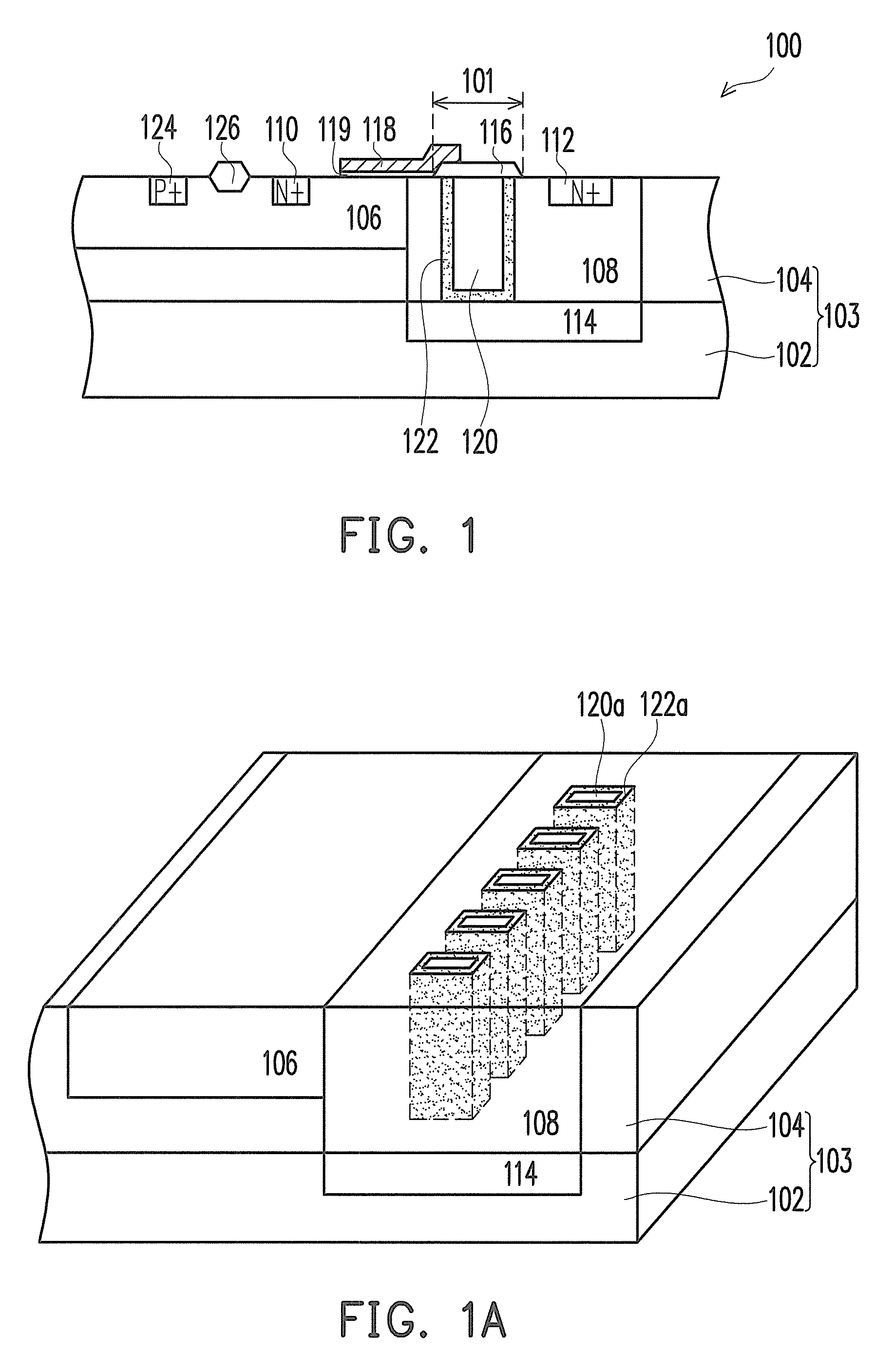
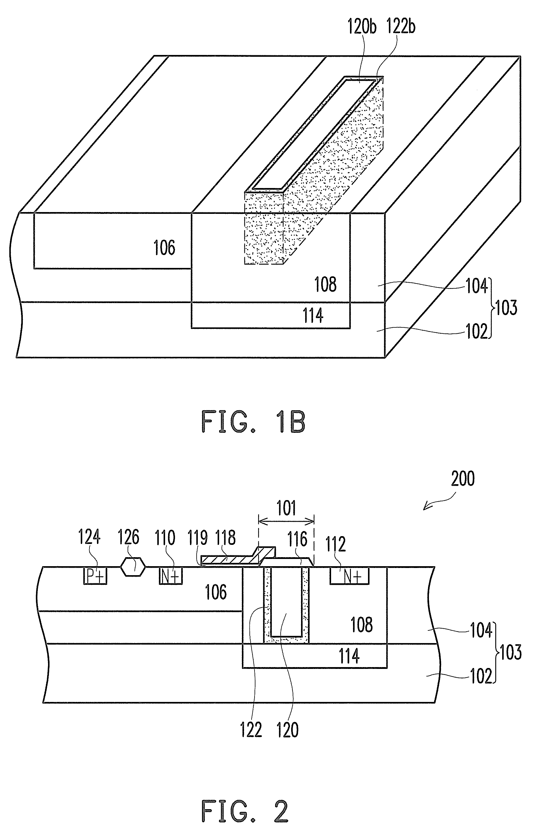
[0038]FIG. 1 is a schematic cross-sectional diagram of an LDMOS device according to an embodiment of the present invention. FIG. 1A is a partial schematic perspective diagram of FIG. 1. For clarity of description, elements such as an isolation structure 116, a gate 118, a gate oxide layer 119, a source region 110, and a drain region 112 are not shown in FIG. 1A.

[0039]Please refer to FIG. 1, an LDMOS device 100 according to the present invention includes a substrate 102 of a first conductivity type, an epitaxial layer 104 of a second conductivity type, a well region 106 of the first conductivity type, a deep well region 108 of the second conductivity type, a source region 110 of the second conductivit...


PUM


Abstract

A reduced surface field (RESURF) structure and a lateral diffused metal oxide semiconductor (LDMOS) device including the same are provided. The RESURF structure includes a substrate of a first conductivity type, a deep well region of a second conductivity type, an isolation structure, at least one trench insulating structure, and at least one doped region of the first conductivity type. The deep well region is disposed in the substrate. The isolation structure is disposed on the substrate. The trench insulating structure is disposed in the deep well region below the isolation structure. The doped region is disposed in the deep well region and surrounds a sidewall and a bottom of the trench insulating structure.

Description

CROSS-REFERENCE TO RELATED APPLICATION[0001]This application claims the priority benefit of Taiwan application serial no. 100115939, filed May 6, 2011. The entirety of the above-mentioned patent application is hereby incorporated by reference herein and made a part of this specification.BACKGROUND OF THE INVENTION[0002]1. Field of Invention[0003]The present invention is related to a semiconductor device, and in particular to a reduced surface field (RESURF) structure and a lateral diffused metal oxide semiconductor (LDMOS) device including the structure.[0004]2. Description of Related Art[0005]In recent years, LDMOS devices have been widely used in all types of power integrated circuits or smart power integrated circuits. Operation of an LDMOS device requires a high breakdown voltage and a low on-state resistance (Ron), so that performance of the device is enhanced. In order to obtain a high breakdown voltage and a low on-state resistance, a type of so-called RESURF LDMOS device is ...

Claims


Application Information

Patent Timeline
IPC IPC(8): H01L29/772H01L29/06
CPCH01L21/26586H01L29/0634H01L29/0649H01L29/0696H01L29/7826H01L29/42368H01L29/66681H01L29/7816H01L29/7817H01L29/0878
Inventor LEE, CHUNG-YEHWU, PEI-HSUNHUANG, SHIANG-WEN
Owner EPISIL TECH
Features
  • R&D
  • Intellectual Property
  • Life Sciences
  • Materials
  • Tech Scout
  • Unparalleled Data Quality
  • Higher Quality Content
  • 60% Fewer Hallucinations
Learn More